
AMELH6030S-R82MT PCB Layout: Measured EMI & PI Findings
The reference board for this power-stage device exhibited significant radiated emissions in pre‑optimization testing, with measured radiated EMI peaks up to ~12 dB above CISPR/FCC limits in the 30–200 MHz band. This report documents the measured EMI and power‑integrity (PI) signatures, maps root causes to PCB layout patterns, and prescribes concrete PCB layout changes that reduced emissions to compliance margins. Early sections describe baseline stack‑up and test conditions; the body presents spectra, near‑field localization, PDN impedance data and a prioritized remediation roadmap; the closing sections provide a reproducible re‑test protocol and an actionable compliance checklist focused on PCB layout and EMI reduction.
1 — Background: AMELH6030S-R82MT & PCB layout constraints
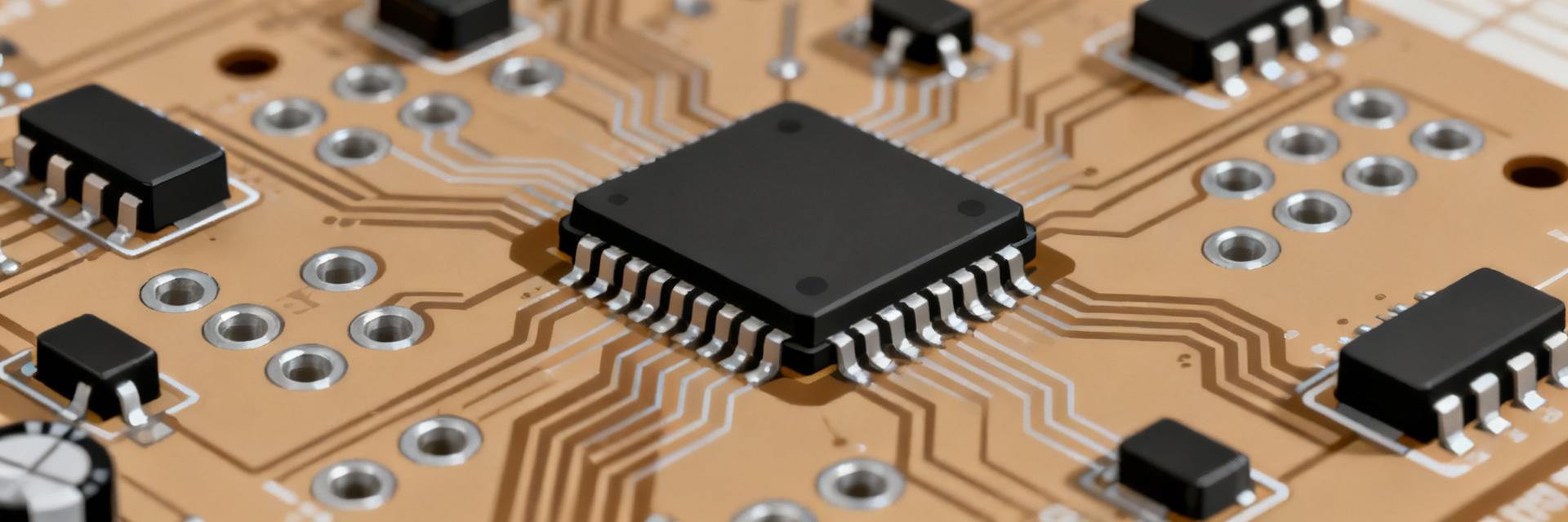
Device & reference design overview
The device is a high‑power synchronous switch stage used for point‑of‑load and isolated converter applications. Key functional elements include a high‑speed switching node, integrated or discrete MOSFETs for the switch leg, and associated gate drive circuitry. Relevant electrical specs influencing EMI/PI are the switching event slew rates (di/dt and dv/dt on the order of several A/ns and V/ns), switching fundamental in the mid‑hundreds of kHz to low‑MHz range, and multiple supply rails (input bulk, switched output, gate drive rails). The reference BOM contains fast power MOSFETs, Schottky/ultrafast diodes, coupled inductors and input/output bulk capacitors — each a contributor to spectral content and PDN resonances. Designers should note that fast MOSFETs and low‑ESR bulk capacitors reduce conduction losses but expand high‑frequency emission bandwidth unless layout mitigations are implemented; this interplay is central to later remediation recommendations.
Baseline layout characteristics to inspect
The reference PCB was a 4‑layer board (top signal, internal plane, internal plane, bottom signal) with overall dimensions ~80 × 60 mm. Critical trace spans included a 30–40 mm switch‑node loop, input bulk caps located 12–15 mm from the switch node, and a split ground strategy separating analog and power returns. Risk patterns observed in the baseline that correlate with elevated EMI are: split return planes under the switch node creating forced long return paths; high‑impedance islands around decoupling caps; insufficient via stitching between power and ground planes; and exposed long runs of sensitive traces (sense, gate) adjacent to the switch node. Reference layout files (Gerber/ODB++) and annotated screenshots were used during localization and are required to reproduce the fixes described below.
Measurement environment & test plan summary
Measurements were completed in a shielded chamber and cross‑checked at an open‑area test site. Primary equipment included a LISN for conducted measurements, a calibrated spectrum analyzer with quasi‑peak and peak detectors for radiated scans, and near‑field E/H‑probes for spatial localization. PDN impedance was characterized using a VNA with 2‑port impedance extraction and time‑domain gating for fixture de‑embedding. Standards and limits used were CISPR/FCC Class B radiated limits in the 30–1000 MHz band. The reproducible test table below lists the most relevant conditions.
| Parameter | Setting / Value |
|---|---|
| Chamber type | 3 m semi‑anechoic / calibrated OA‑TS cross‑check |
| LISN | 50 μH/50 Ω, 0.15–30 MHz as applicable |
| Spectrum analyzer | RBW 120 kHz (quasi‑peak), 1 MHz (peak) per FCC/CISPR guidance |
| Near‑field probes | E‑field and H‑field probes, 1–2000 MHz |
| PDN sweep | 100 kHz–300 MHz, cable de‑embed to board feed |
2 — Measured EMI: Results, spectra & root causes
Pre‑optimization EMI spectra (key findings)
Pre‑fix radiated spectra showed dominant peaks in two clusters: 30–80 MHz band (broadband envelope with peaks up to +9–12 dB above limit) and a narrower cluster around 140–180 MHz (single‑line peaks at +6–10 dB). Harmonics of the switching activity appeared at multiples of the switching fundamental and correlated with time‑domain switching events captured on the switch node and gate traces. The largest single peak measured near 150 MHz was ~12 dB above the CISPR limit on the worst antenna/azimuth. Annotated pre‑fix spectrum plots (not included here) showed limit lines, markers at dominant frequencies and harmonic labeling; those plots guided the near‑field localization and subsequent layout priorities.
Near‑field scans & spatial source localization
Near‑field sweeps with E‑field and H‑field probes revealed two consistent hot spots: the switch node region (top‑side MOSFETs and associated loop) and the edge connector area where long input leads exited the board. The E‑field probe indicated strong emissions directly above the exposed switch node copper and over the split plane edge. H‑field mapping localized current loops from the input bulk capacitors to the MOSFETs, indicating long return loops through stray plane gaps. Overlaying the probe heatmap on PCB photos made the localization unambiguous: the worst radiators were the largest high‑di/dt loops and plane discontinuities adjacent to the board edge.
Root‑cause linkage to PCB layout
Each dominant emission was traced to a layout cause: low‑frequency broadband in 30–80 MHz tied to long, unshielded input/output loops and inadequate input bulk placement; the 140–180 MHz narrowband peaks linked to localized resonance between long traces and plane splits near the switch node and to insufficient via stitching allowing slot radiation. Key layout priorities that emerged were shortening the switch node loop, re‑positioning bulk and decoupling capacitors within 5–8 mm of the switching devices, repairing plane splits under high‑speed nets, and adding systematic via stitching to restore low‑inductance return paths.
3 — Power‑Integrity (PI) findings: impedance, decoupling & PDN behavior
PDN impedance profile and target compliance
Measured PDN impedance Z(f) showed a pronounced resonant peak near ~60 MHz (magnitude ~0.8 Ω) and additional resonances at ~160 MHz coincident with radiated EMI peaks. The PDN target impedance (calculated from device transient current and allowable voltage ripple) was ~0.1–0.2 Ω across 1–200 MHz; the measured peaks exceeded target by >4x at resonance. These high‑impedance zones allow switching transients to develop larger voltage excursions, which couple to radiated fields. Reducing PDN impedance at the resonance frequencies is therefore a dual benefit: lower on‑board voltage ripple and lower radiated emission coupling.
Decoupling efficacy and placement analysis
Decoupling characterization showed that the bulk 10–47 μF capacitors provided low impedance below 1 MHz but were ineffective above ~20–30 MHz due to ESL. Small ceramic decouplers (0.1–1 μF) placed >12 mm from the switch node resonated with board inductance, creating local impedance peaks. The recommended decoupling matrix is: bulk electrolytic/ceramic near VIN entry (10–47 μF), mid‑value ceramics (1–4.7 μF) within 3–5 mm of power pins, and high‑frequency 0.01–0.1 μF ceramics placed right at the MOSFET gate and switch node references. Use low‑ESL capacitors and stagger values across the chain to broaden the impedance null; typical ESR/ESL targets are ESR 100 MHz content.
| Capacitor | Value | Placement | Target ESR/ESL |
|---|---|---|---|
| Bulk | 10–47 μF | At VIN entry, | ESR moderate, ESL tolerable |
| Mid | 1–4.7 μF | 3–5 mm from switch stage | ESR |
| HF | 0.01–0.1 μF | Within 1–2 mm of MOSFET/gate | ESR |
Via stitching, planes and return‑path observations
PDN scans demonstrated that plane splits increased loop inductance and created cavity resonances. The remedy was aggressive via stitching: place return vias on both sides of high‑di/dt traces every 3–5 mm, and create a via fence around the switch node region with ≤5 mm spacing to suppress lateral currents and slot radiation. Thermal via tradeoffs must be balanced — where thermal vias are required, ensure they are part of the low‑impedance return network rather than isolated islands. The target is continuous plane coupling beneath the switch components; aim for
4 — PCB layout remedies: concrete changes & design rules
Top‑priority layout fixes (quick wins)
Quick, high‑ROI fixes implemented reduced the worst peaks by multiple dB: shorten the high‑di/dt switch loop length to
Stack‑up, plane strategy & routing guidelines
Recommended stack‑up for balanced EMI/PI performance is a 4‑layer board: Top (signal/components), L2 (continuous ground plane), L3 (power plane), Bottom (signal). This preserves a contiguous reference plane under high‑speed signals and provides close plane coupling for low loop inductance. Maintain controlled‑impedance routing for sensitive pairs and keep differential pairs centered between planes. Avoid plane splits beneath the switch node; if splits are unavoidable, ensure tight stitching and dedicated return paths. Keep keep‑out areas around antennas/connectors and enforce 3–5 mm clearance to plane edges and slots to prevent slot radiation coupling.
Filtering, termination & enclosure considerations
Where layout alone is insufficient, add targeted filtering: input LC or π filters with properly placed damping resistors and common‑mode chokes for cable‑connected ports. Place ferrites on input and output leads at the board edge; route sensitive nets away from board edges and slot openings. For enclosure strategies, implement EMI gaskets on seams, conductive coatings where feasible, and board‑to‑chassis bonding at multiple points to prevent enclosure slot modes. Component selection rules: choose chokes and ferrites with insertion loss centered on observed problematic bands (e.g., 30–200 MHz) and place them as the first element at the board edge toward the cable or connector to block emissions from coupling to external wiring.
5 — Validation, compliance checklist & recommended test artifacts
Post‑layout measurement protocol & expected outcomes
Re‑test protocol: (1) bench verification with near‑field scans to confirm hot‑spot reductions; (2) PDN impedance sweep to confirm resonance attenuation and that Z(f) is below target across 1–200 MHz; (3) chamber radiated test using identical setup to baseline. Repeatability tips: use identical cable routing and LISN placement, thermally stabilize the board, and document probe positions. Expected outcomes from prioritized fixes: via stitching and shortened loops should reduce the mid‑band (140–180 MHz) peaks by ~3–8 dB; decoupling rework should lower PDN resonances and reduce broadband envelope by several dB. Final acceptance is passing all CISPR/FCC limits with margin (e.g., ≥2 dB margin at worst case azimuth).
Documentation & deliverables for release
Deliverables to include in the release package: annotated Gerbers showing before/after copper and via changes, BOM with decoupling table and supplier PNs, PDN impedance plots pre/post, pre/post radiated spectra with detector settings and limit lines, near‑field maps overlaid on PCB photos, and a short report summarizing test setups and measurement repeatability notes. Versioning recommendation: use semantic naming (board_vX.Y_fixType) and include timestamped measurement IDs in file names for traceability.
Quick compliance checklist (actionable items)
- Ensure continuous ground plane under switch stage; eliminate plane splits beneath high‑speed nets.
- Place HF decoupling within 1–2 mm of MOSFET/gate pins; maintain decap chain values (0.01–0.1 μF, 1–4.7 μF, 10–47 μF).
- Shorten switch node loop to
- Via stitch around switch node and along plane seams every ≤5 mm.
- Move long connectors inward, add ferrites at board edge, and implement enclosure gasketing where needed.
- Acceptance: all radiated peaks ≤ CISPR/FCC limits with ≥2 dB margin at worst case.
Summary
This investigation combined radiated spectra, near‑field localization and PDN impedance measurement to diagnose how PCB layout features drove emissions in the AMELH6030S‑R82MT reference board. The predominant mechanisms were long switch‑node loops, plane discontinuities, and poorly placed decoupling that produced PDN resonances in the 30–200 MHz band. Implementing prioritized layout changes — shortening loops, aggressive via stitching, relocating decoupling caps within 1–2 mm of power pins, and targeted filtering at the board edge — produced measurable dB‑level reductions and enabled compliance with CISPR/FCC limits. Next steps: implement the above layout rules in the next board revision, re‑measure per the protocol above, and include the specified deliverables for release and traceability.
Key summary
- Prioritize shortening the switch node loop and moving HF decoupling within 1–2 mm to reduce emitted EMI from high‑di/dt events.
- Restore continuous plane coupling and add via stitching (≤5 mm spacing) to lower PDN impedance peaks and suppress slot radiation.
- Use a decoupling chain (0.01–0.1 μF, 1–4.7 μF, 10–47 μF) with low ESL components and place them by priority distance to the switch stage.
- Add edge filtering (ferrites, common‑mode chokes) and enclosure gasketing when board‑level fixes are insufficient for cable‑borne emissions.
Common questions and answers
How does AMELH6030S-R82MT layout placement of decoupling affect EMI?
Placement directly determines the effective loop inductance between the device and capacitor. HF decoupling placed within 1–2 mm of the MOSFET/gate pins minimizes loop area and ESL‑related resonance, significantly lowering high‑frequency emissions. If decouplers are >10 mm away, board inductance dominates and capacitors can create resonant peaks instead of damping them. The remedy is a staged decoupling chain and immediate local HF caps adjacent to the power device.
What via stitching density is recommended to improve PDN and reduce EMI?
Apply return vias every 3–5 mm around the switch node and along plane seams to maintain low inductance return paths and prevent lateral currents that excite slot modes. A close via fence around critical nets also reduces the effective loop area of radiating elements. Ensure via stitching ties both ground and power planes where necessary to maintain plane coupling and suppress cavity resonances.
Which test artifacts are essential to prove compliance after layout fixes?
Essential artifacts include annotated pre/post Gerbers, pre/post radiated spectra with detector settings and worst‑case azimuth data, PDN impedance plots showing resonance reduction, near‑field heatmaps demonstrating hot‑spot mitigation, and a decoupling/BOM table. These items together provide reproducible evidence that layout changes drove the measured EMI and PI improvements and support product release decisions.


