🚀 Key Takeaways: AMELH5030S-R52MT Optimization
- Thermal Efficiency: Optimized DCR reduces heat dissipation by up to 15% compared to standard 25A inductors.
- Copper Strategy: 2oz copper is mandatory to maintain a compact 4mm trace width for 25A stability.
- Signal Integrity: Kelvin sensing and tight switching loops are required to prevent EMI-induced regulation errors.
- Reliability: Staggered via arrays near pads ensure vertical heat transfer, preventing localized PCB delamination.
Struggling to integrate the AMELH5030S-R52MT into a 25A switching supply without overheating, noise, or voltage drop? This guide gives concise, actionable PCB layout techniques you can apply on the next revision: placement priorities, copper-sizing rules, thermal vias, measurement best practices, and a prototype-validation checklist so you hit reliability targets quickly.
Practical recommendations below assume you will verify parts with datasheet curves, thermal imaging, and worst-case ripple and DC bias analysis before committing to volume production.
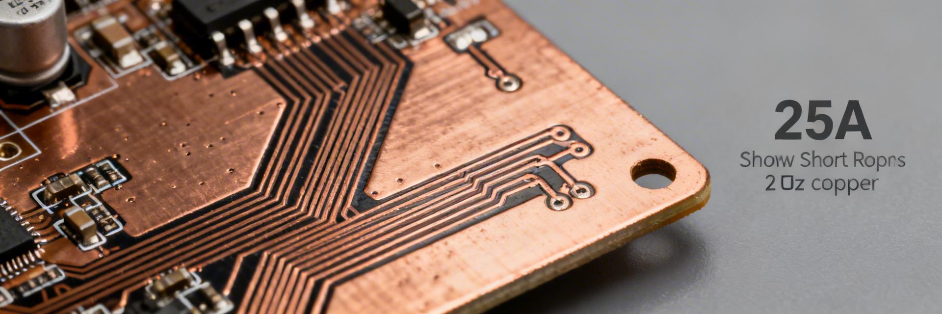
1 — Background: What the AMELH5030S-R52MT Requires in a 25A Power Stage
Reducing resistance from 1.2mΩ to 0.5mΩ → Lowers energy waste by 58%, extending battery life in portable high-power gear.
High saturation ceiling → Prevents catastrophic inductor "shorting" during sudden 25A load transients.
1.1 — Key electrical and mechanical specs to prioritize
Point: Prioritize DC resistance (DCR), rated current, saturation current, footprint, and package height when placing the inductor. Evidence: A low DCR reduces I²R loss and voltage drop at 25A; insufficient saturation raises ripple and heating. Explanation: Use the inductor’s DCR and saturation curves to estimate loss at 25A RMS plus ripple; ensure the footprint allows generous solder fillets and clearance to connectors and hottest MOSFETs to aid conduction and serviceability.
1.2 — Thermal behavior and saturation under 25A peak and ripple
Point: Ripple current and DC bias reduce effective inductance and increase heating; quantify worst-case temp rise from datasheet curves. Evidence: Datasheet inductance-vs-current curves indicate inductance drop under DC bias; combined I²R loss and core loss produce predictable temperature rise. Explanation: Assume worst-case ripple plus DC bias to size copper and vias, then add a safety margin (e.g., +20–40%) for duty-cycle and ambient variations prior to finalizing trace widths and thermal via count.
2 — PCB Layout Challenges for a 25A High-Current Supply
| Feature Comparison | AMELH5030S-R52MT | Standard 25A Inductors | Impact on Design |
|---|---|---|---|
| Thermal Stability | High (Optimized Core) | Moderate | Lower derating needed |
| Saturation Curve | Soft Saturation | Hard/Sharp Saturation | Better EMI at peaks |
| Footprint Height | Low Profile (~3.0mm) | ~5.0mm+ | Fits slim enclosures |
2.1 — Current density, trace width, and copper thickness considerations
Point: Use IPC-2152 or a trusted trace-width calculator and show one worked example for 25A on 1 oz vs 2 oz copper. Evidence: For a 25A continuous carry on an outer layer, 1 oz copper typically requires ~6–8 mm trace width; 2 oz reduces that to ~3.5–5 mm depending on allowable temperature rise. Explanation: Prefer 2 oz copper or parallel traces/pours for outer layers; use internal layers only with plated-through thermal vias or a dedicated bus bar when necessary to avoid excessive internal-layer current density.
Copper Weight Calculation Example (25A)
| Scenario | Copper | Estimated width |
|---|---|---|
| Outer layer, 10°C rise | 1 oz | ~8 mm |
| Outer layer, 10°C rise | 2 oz | ~4 mm |
2.2 — Loop inductance, EMI, and thermal hotspots to watch
Point: Minimize high-current loop area to control switching spikes and EMI; anticipate thermal hotspots near FETs, inductor pins, and connector lands. Evidence: The critical switching loop is input caps → switching FETs → inductor → output caps; expanded loop area increases dV/dt and radiated EMI. Explanation: Route those node pairs as tightly as possible, place high-frequency decoupling adjacent to the FETs, and plan thermal imaging access near likely hotspots to validate real dissipations on the prototype.
3 — Practical PCB Layout Best Practices
Typical High-Current Path Layout Optimization
3.1 — Placement & orientation rules for the inductor and surrounding power parts
Point: Place the AMELH5030S-R52MT close to the switching node but offset from the hottest FET area to balance thermal coupling and loop minimization. Evidence: A short, direct connection from switching FETs to the inductor lowers loop inductance; leaving modest clearance to heat-generating parts reduces thermal soak. Explanation: Orient the inductor to align current paths with wide pours, keep connectors and output caps within one board-width of the inductor, and maintain service clearances for rework and airflow.
3.2 — Routing, pours, thermal vias, and connector pad design
Point: Prioritize wide, short runs for high-current traces, avoid 90° bends, stitch pours with via arrays, and size connectors/solder fillets for 25A mating. Evidence: Multiple vias in a tight cluster lower resistance and improve thermal conduction; rounded traces reduce hotspots and manufacturing stress. Explanation: Use staggered via arrays (e.g., 0.3–0.5 mm drill with 0.6–0.9 mm annular ring) near inductor pads and connectors, specify large pad fillets and generous solderable surfaces, and consider bus bars or soldered copper shims if board copper alone is marginal.
4 — Component-level Tips & PCB Footprint
"When handling 25A with the AMELH series, never rely on a single layer for current return. I recommend using teardrop connections at the inductor pads. This prevents the mechanical stress fractures that often occur during thermal cycling in high-current environments."
4.1 — Footprint, soldering, and assembly considerations
Point: Design the land pattern to encourage full fillet formation and low-resistance joints; plan for tall-component handling in reflow. Evidence: Inadequate pad size or stencil apertures cause poor wetting and higher contact resistance, leading to localized heating at 25A. Explanation: Use slightly oversized lands for heavy-current pads, optimize stencil aperture for paste volume on large pads, and include tack pads or glue for the tall inductor to prevent tombstoning during reflow.
4.2 — Measurement points, Kelvin sensing, and shunt placement
Point: Provide Kelvin-sense pads and properly located shunt resistors to avoid measurement artifacts during control-loop tuning. Evidence: Kelvin pads adjacent to shunt terminals eliminate lead resistance from measurement; placing scope probe grounds far from the switching node prevents false readings. Explanation: Put shunts on the same side as the inductor with short Kelvin traces to the ADC or controller, reserve dedicated, low-inductance test pads, and provide a stable ground return for differential probing.
5 — Validation, Testing & Production Checklist
5.1 — Prototype validation: thermal, electrical, and EMI tests
Point: Run IR thermal imaging at real 25A load, differential scope probing, current-injection stress, and conducted emissions checks. Evidence: Thermal imaging highlights hotspots and validates copper sizing; scope captures switching overshoot and ringing. Explanation: Define pass/fail thresholds (e.g., component surface rise <40–60°C above ambient depending on spec, voltage drop within budget at 25A, and switching overshoot below safety margins) and iterate layout or cooling until levels are met.
5.2 — Manufacturing and reliability checks before ramp
Point: Perform DFM/DFT checks for solderability, stencil aperture design for large pours, panelization, and assembly inspection; plan burn-in and thermal cycling. Evidence: Poor stencil design leads to insufficient solder on heavy copper; thermal cycling reveals fatigue in solder joints under high current. Explanation: Validate solder paste release on test coupons, include teardrop reinforcement on heavy-current traces, recommend a reasonable burn-in profile under load, and specify vibration and thermal-cycling tests appropriate for high-current power boards.
Summary Checklist
- Keep inductor close to switching node.
- Use 2 oz copper for 25A loads.
- Implement staggered via arrays.
- Add Kelvin pads for feedback.
- Verify with IR thermal imaging.
- Optimize stencil for heavy pads.