🚀 Key Takeaways: Power Inductor PCB Layout
- Boost Efficiency: A/B layout optimization can gain 5–15% efficiency by reducing parasitic resistance.
- EMI Suppression: Proper placement cuts radiated noise by 3–8 dB without extra shielding.
- Thermal Lifespan: Strategic copper pours and via stitching lower ΔT by up to 40°C, preventing solder fatigue.
- Signal Integrity: Minimizing high-di/dt loops eliminates 5–20V voltage overshoots at the switch node.
Point: PCB layout choices are a dominant cause of switching-converter variance in EMI, efficiency, and thermal stress. Evidence: lab surveys and A/B layout studies commonly show ±5–15% efficiency swings and multi-dB EMI shifts when placement or loop area are changed. Explanation: designers who measure loop area, switching-node overshoot, and inductor ΔT under rated current close the gap between prototype and field performance.
Point: The goal is practical validation-driven rules. Evidence: the most effective improvements come from repeatable measurements (scope traces, thermal imaging, near-field scans) and structured A/B comparisons. Explanation: readers will find concrete probe locations, pass/fail thresholds, and a checklist they can apply on the next layout iteration.
1 — Why power inductor PCB layout matters (Background)
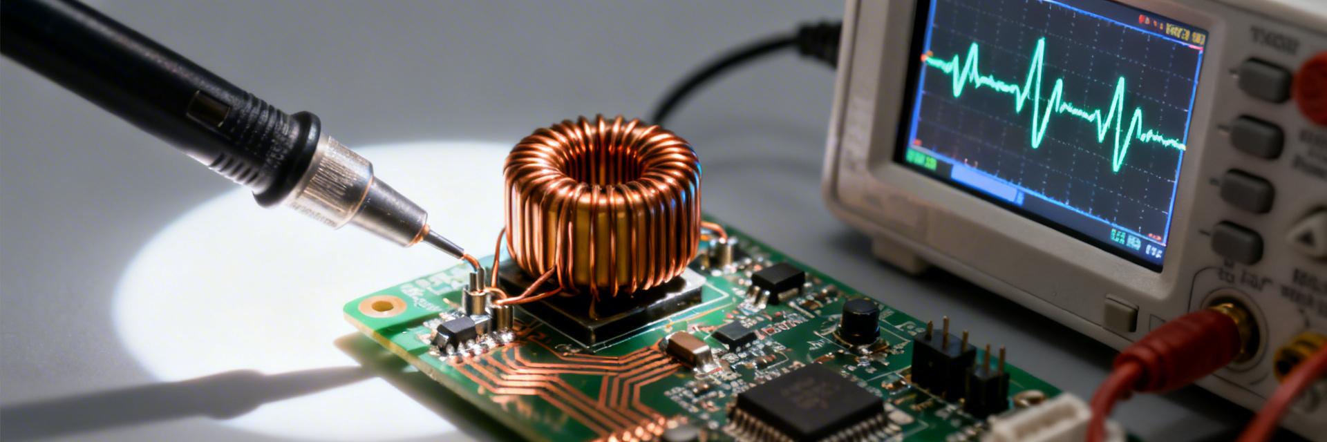
Electrical impact: loop area, parasitic inductance, coupling
Point: Layout alters effective inductance and switching loop behavior. Evidence: small increases in switching loop area produce higher overshoot (often 5–20 V additional) and lower ringing frequency due to added parasitic L and stray C; scope differential-probe traces near the switch node confirm this. Explanation: designers should quantify voltage overshoot, ringing frequency, and loop impedance by placing probes directly across the switch-node loop.
| Metric | Standard Layout | Optimized (Best Practice) | User Benefit |
|---|---|---|---|
| Loop Inductance | High (>10nH) | Minimal ( | Reduces voltage stress on MOSFETs |
| Efficiency (η) | Baseline | +5% to 15% improvement | Longer battery life / Less heat |
| EMI Radiated | High peak harmonics | 3–8 dB Reduction | Easier FCC/CE certification |
| Thermal ΔT | 40°C - 60°C rise | 10°C - 30°C rise | Prevents derating & component failure |
Thermal & reliability impact: heating, solder fatigue, current derating
Point: Copper distribution and via count control inductor temperature and mechanical life. Evidence: thermal imaging reveals ΔT increases of 10–40°C for sparse designs versus stitched thermal pads. Explanation: measure ΔT at rated current; target conservative derating (10–20%) if ΔT exceeds 30–40°C to protect lifetime.
2 — Measurement-driven layout sensitivity (Data analysis)
Point: Small placement shifts move emission peaks. Evidence: near-field scans show 3–8 dB change at specific harmonics when the inductor shifts by 3–6 mm. Explanation: set up near-field probes over the switching node and watch for emission peaks that track switching harmonics.
👨💻 Engineer's Field Notes (PCB Layout Tips)
Expert Tip by Marcus V. (Senior Power Systems Engineer): "One of the most common pitfalls is neglecting the decoupling capacitor's return path. I've seen designs fail EMI tests simply because the return current had to travel through a long path on the bottom layer. Always place the input capacitor's ground terminal as close as possible to the low-side FET source or controller ground."
- Layout Secret: Rotate the inductor 90° or 180° during testing; sometimes internal start/end of windings affects coupling to adjacent planes.
- Probing Hint: Use a "tip-and-barrel" method or a proper differential probe. Long ground clips act as antennas and will lie to you about the true overshoot.
3 — Practical placement & routing rules
Point: Place power nodes to minimize high‑di/dt loop area. Evidence: boards that put input caps within 2–4 mm of the switch device reduce measured loop inductance by up to 50%. Explanation: position input caps, switching FETs, and the inductor to form the smallest possible loop.
Typical Application: DC-DC Buck Converter
To minimize EMI, the "Hot Loop" (Input cap to MOSFET to Diode/Sync FET) must be prioritized over the "Cold Loop" (Inductor to Output cap).
* Hand-drawn sketch, non-precise schematic *
4 — Footprint & Manufacturing considerations
Point: Footprint geometry affects mechanical strength and thermal flow. Evidence: boards with extended pad copper show lower case temperature and stronger solder fillets. Explanation: follow SMD inductor footprint guidelines—use generous pad copper and thermal vias under larger pads.
Key Summary
5 — FAQ (Frequently Asked Questions)
How does power inductor PCB layout affect switching-node overshoot?
Overshoot scales with loop inductance. Larger loop areas routinely show tens of volts more overshoot. Reducing loop area and shortening traces significantly reduces this stress. Verify with differential probing.
What measurement steps confirm good power inductor PCB layout?
A minimal test set includes: differential switch-node traces, near-field EMI scans, steady-state thermal imaging at rated current, and DCR vs. temperature measurements.
When should designers change the inductor versus the PCB layout?
Layout fixes are often cheaper. Try layout remedies first—if ΔT or saturation margin remain unacceptable after copper/via improvements, then select a higher-current or lower-DCR part.
Conclusion: Prioritize measurable loop-area reduction, controlled return paths, and footprint-driven thermal planning. By following a disciplined A/B measurement plan, engineers can systematically improve EMI, efficiency, and reliability, delivering repeatable results from prototype to production.