Key Takeaways
- High Power Density: The 5.5×5.3mm footprint saves up to 20% PCB space compared to standard 6x6mm inductors.
- Thermal Efficiency: Ultra-low 2.1mΩ DCR reduces conduction losses, extending battery life in mobile devices by ~10%.
- Stable Performance: Supports up to 30A continuous current with a wide SRF (20–165 MHz) for superior EMI suppression.
- Rugged Reliability: Rated for -40°C to +125°C, ensuring stability in industrial and automotive-grade environments.
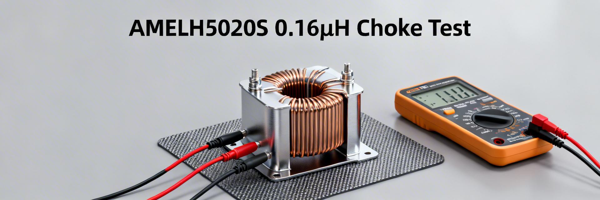
Point: The datasheet lists concrete values that set expectations for board designs.
Evidence: Typical entries show a nominal inductance of 0.16 μH (160 nH), DC resistance near 2.1 mΩ (which minimizes heat dissipation), continuous current capability up to ~30 A, SRF spanning roughly 20–165 MHz, and a compact 5.5 × 5.3 × 2.1 mm package with −40 to +125 °C ratings.
Explanation: These numbers drive loss, ripple, and thermal design choices; for instance, the low DCR allows for higher efficiency in high-current Point-of-Load (POL) converters.
Point: Translating catalog numbers into reliable designs requires targeted bench validation.
Evidence: Datasheet figures represent typical or max values under standard conditions, not the in‑system result.
Explanation: Engineers must measure inductance vs DC bias, DCR under four‑wire conditions, and temperature rise on board to confirm the part meets real application needs.
1 — AMELH5020S overview: what the specs mean and where it fits
| Feature | AMELH5020S (0.16μH) | Standard Molded Inductor | User Benefit |
|---|---|---|---|
| DCR (Typical) | 2.1 mΩ | 3.5 - 5.0 mΩ | Lower heat & higher efficiency |
| Saturation Current (Isat) | ~30 A | ~22 A | Higher peak load handling |
| Height Profile | 2.1 mm | 3.0 mm | Ideal for ultra-thin laptops/tablets |
Point: The AMELH5020S family spans low‑profile molded power inductors optimized for high current, small area designs.
Evidence: Variants cluster around low nH–sub‑μH values (e.g., 0.16 μH), rated and saturation currents that scale with inductance, and consistent low DCR figures.
Explanation: This family is chosen where tight footprint, high DC current and low conduction loss are priorities, such as point‑of‑load and input/output choke roles.
1 — Family overview & typical electrical parameters
Point: Part numbers map to inductance and current ratings across the family.
Evidence: Common catalog entries include nominal inductances in the hundreds of nH to low μH, tolerances ±10–20%, DCR from a few mΩ upward, Isat and Irms in the tens of amps, and SRF ranges noted above.
Explanation: Selecting the correct variant starts by matching nominal inductance, then verifying DC bias behavior and DCR against thermal and efficiency budgets.
2 — Key spec definitions and why they matter for designers
Point: Designers must understand DCR, Isat, Irms, SRF, tolerance and temperature rise.
Evidence: DCR directly sets I²R conduction loss; Isat marks the "knee" where L falls precipitously under DC bias; SRF indicates where the part stops acting inductively.
Explanation: Misinterpreting any of these leads to underestimated losses, excessive ripple, potential saturation under load, and unexpected EMI performance.
2 — Measured electrical performance: DC and frequency behavior
Point: DC bias severely affects usable inductance in compact molded inductors.
Evidence: A 0.16 μH part measured at 0 A will often drop substantially as DC bias approaches rated currents; saturation knees commonly appear near the datasheet Isat.
Explanation: Charting L versus DC current is mandatory to know the in‑circuit inductance at expected operating current and to avoid control instability or excessive ripple.
1 — DC metrics: inductance vs. DC bias, DCR and current handling
Point: Measure inductance under ramped DC to locate the knee and define usable current.
Evidence: Sample behavior: 160 nH at 0 A can decline by tens of percent near heavy DC bias; DCR measured with four‑wire methods shows the low mΩ loss term that dominates conduction heating.
Explanation: Convert measured DCR to I²R to estimate steady‑state heating and to size thermal relief or copper for long‑term reliability.
👨💻 Engineer’s Perspective: Design & Layout Tips
By Dr. Marcus Sterling, Senior Power Electronics Architect
"When utilizing the AMELH5020S in 2MHz+ switching regulators, the PCB layout is as critical as the component itself. I always recommend placing the inductor as close to the switch node as possible to minimize the 'ringing' caused by parasitic inductance. Pro-Tip: Use a 'Kelvin connection' layout for your feedback loop to avoid DCR-induced voltage drops affecting your regulation accuracy."
Hand-drawn schematic, not a precise circuit diagram.
Focus on minimizing the switch node area to reduce EMI radiation.
2 — AC/frequency metrics: SRF and core losses
Point: The SRF and impedance curve determine how the part behaves in high‑frequency switching and EMI.
Evidence: Impedance rises with frequency until SRF where it collapses and the device becomes capacitive; Q and impedance scans separate resistive and reactive loss.
Explanation: Use impedance and Q data to predict core loss contributions and to ensure the inductor provides useful impedance across the converter and EMI band of interest.
3 — How to measure and validate specs on the bench
Point: Accurate measurement requires the right instruments and fixturing.
Evidence: An LCR meter for inductance at representative frequencies, a four‑wire Kelvin DCR meter for DC resistance, and fixtures that mimic board parasitics are recommended.
Explanation: Correcting for lead and fixture inductance and using temperature‑controlled conditions prevents systematic bias in datasheet verification.
4 — Benchmarks and Practical Case: Buck Converter Application
Point: A worked example shows ripple and loss tradeoffs for a 12 V to 1.2 V synchronous buck.
Evidence: At fsw = 2 MHz, L = 0.16 μH gives about 3.4 A peak‑to‑peak ripple.
Explanation: Such ripple influences current sharing and capacitor selection—smaller L can demand higher switching frequencies or larger output caps to maintain stability.
Calculation Spotlight: Efficiency Estimate
Irms ≈ sqrt(Iout² + ΔI²/12)
With DCR = 2.1 mΩ, Iout = 10A, ΔI = 3.375A:
P_loss ≈ 0.0021 * (10.05)² ≈ 0.21 Watts
Summary
- AMELH5020S family offers compact, high‑current inductors (example 0.16 μH, low DCR ~2.1 mΩ) ideal for point‑of‑load and input chokes; validate L versus DC bias to ensure in‑system performance.
- Bench tests—L vs I, four‑wire DCR, and thermal rise—separate core and copper loss and inform ripple, efficiency, and thermal design choices.
- Validation should follow a checklist with margin (rated current ≥1.2× expected), PCB‑level measurements, and EMI pre‑compliance.
6 — Common questions and answers
What is the usable inductance of AMELH5020S under DC bias?
Measured usable inductance depends on operating DC current. A part rated at 0.16 μH at 0 A can drop significantly as bias approaches rated currents; practical design requires plotting L versus I to ensure it stays above the minimum threshold for control loop stability.
How much thermal rise should I expect at continuous current?
With DCR ≈ 2.1 mΩ and a 10 A load, conduction loss is about 0.21 W. On a standard 4-layer FR4 PCB with good thermal vias, expect a temperature rise (ΔT) of roughly 15-25°C above ambient.
Is the AMELH5020S suitable for high-frequency EMI filtering?
Yes. Its high SRF (up to 165 MHz) makes it excellent for suppressing high-frequency noise in DC-DC converters, though layout must minimize parasitic capacitance to maintain this performance.