Professional Technical Analysis & Specification Guide
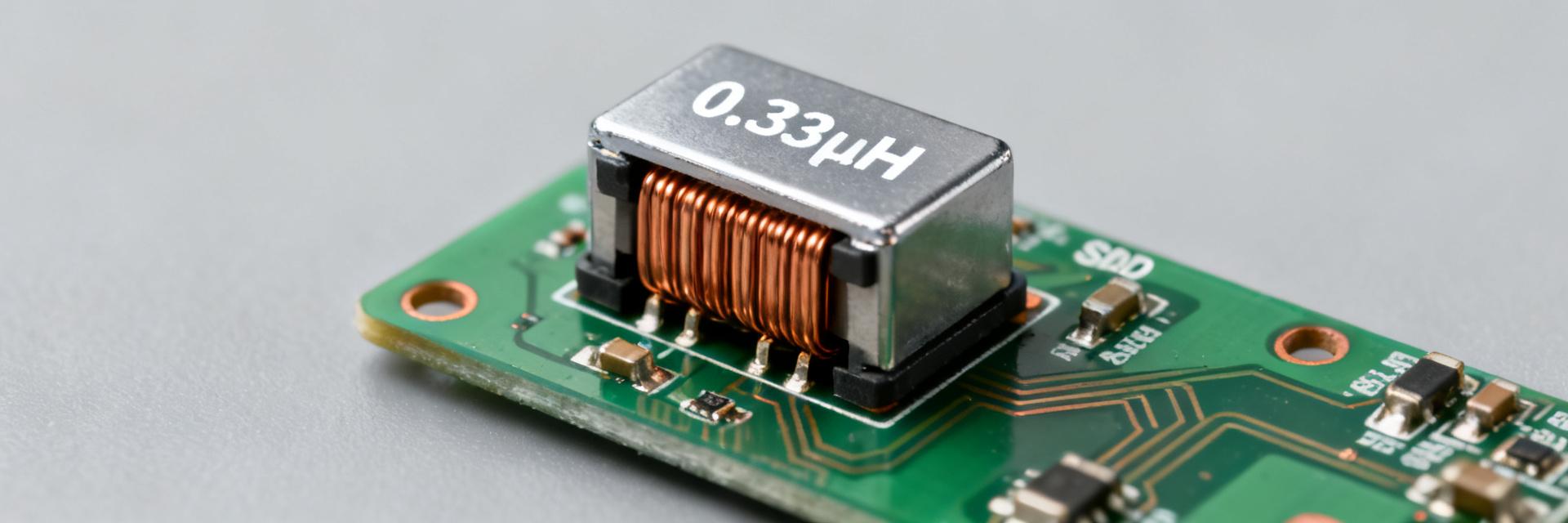
Point: The AMELH5030S-R33MT is a compact 0.33 µH SMD power inductor built for high-current DC–DC and power-filtering roles.
Evidence: The part comes in a 5.5 × 5.3 × 3.1 mm package with an on-board operating limit to 125°C and a storage range down to −40°C.
Explanation: These mechanical and thermal bounds make it suitable for tight point-of-load designs where board space and thermal margin are constrained.
Point: This article provides a concise, data-driven breakdown of specs, measured behavior, and test methods.
Evidence: Coverage includes inductance vs frequency, DCR, Irms/Isat interpretation, thermal rise testing, and practical layout guidance tied to standard measurement practice.
Explanation: Engineers will get actionable selection checks and reproducible test formats to validate performance before deployment.
1 — Background: What the AMELH5030S-R33MT is and where it fits
1.1 — Core physical & electrical identifiers
Point: The device designation and primary electrical figures define fit and function. Evidence: Nominal inductance is 0.33 µH in a 5.5 × 5.3 × 3.1 mm SMD package; RoHS-compliant construction is noted in the official datasheet. Explanation: These identifiers guide footprint planning, thermal allowance, and whether the part meets board-level compliance and process limits for reflow and assembly.
1.2 — Typical application spaces
Point: The 0.33 µH value targets modern switching power stages. Evidence: Common uses include synchronous buck converters, point-of-load filters, EMI suppression on power rails, and high-frequency switching applications. Explanation: Designers choose this inductance to balance ripple current handling against size and DCR, making it a common choice where switching frequencies are high and space is limited.
2 — Electrical performance & core specs (data analysis)
| Parameter | Value (Nominal) | Unit |
|---|---|---|
| Inductance | 0.33 | µH |
| Dimensions | 5.5 × 5.3 × 3.1 | mm |
| Operating Temp | Up to +125 | °C |
2.1 — Inductance, tolerance and frequency behavior
Point: Inductance nominal and frequency response determine usable bandwidth. Evidence: The nominal 0.33 µH value will shift with frequency; self-resonant frequency defines the upper usable range per manufacturer curves. Explanation: Understanding inductance vs frequency (and SRF) is essential when the inductor sits near switching harmonics—designers should consult the official datasheet or bench L(f) plots when targeting MHz-range switching.
2.2 — DCR, rated current (Irms) and saturation current (Isat)
Point: DCR and current ratings drive loss and thermal budget. Evidence: Low DCR reduces conduction losses but must be balanced against core geometry that sets Isat; Irms rating reflects allowable steady current before excessive temperature rise. Explanation: Selection should use Irms and Isat with safety margin—if peak currents approach Isat, expect inductance collapse and degraded regulation under load.
3 — Thermal, reliability & environmental specs (data analysis)
3.1 — Temperature limits, thermal rise and derating
Point: Thermal behavior under load determines long-term reliability. Evidence: On-board operating limits are typically up to 125°C; temperature rise vs current curves indicate how much steady current elevates junction/ambient. Explanation: Designers must derate Irms relative to ambient temperature and nearby heat sources; use thermal probes or IR mapping to validate steady-state temperatures on the actual PCB.
3.2 — Reflow, solderability and lifecycle considerations
Point: Assembly profiles and solder joint robustness affect lifecycle. Evidence: Reflow peak temperatures and allowable reflow counts are specified in the datasheet; correct pad geometry and cleaning processes preserve solderability. Explanation: Follow recommended reflow profiles and avoid excessive mechanical stress during board handling to maintain long-term electrical and mechanical integrity.
4 — How to test and measure key specs (method guide)
4.1 — Practical test setups for L, DCR, Isat and Irms
Point: Reproducible measurements require specific instruments and fixturing. Evidence: Typical instruments include an LCR meter for L at defined frequencies, Kelvin DCR meter, a programmable current source for Isat ramps, and thermal probes for Irms thermal testing. Explanation: Use short Kelvin leads or a dedicated PCB test fixture to avoid measurement artifacts; perform saturation tests by ramping DC current while monitoring inductance drop.
4.2 — Test reporting format and what to include
Point: Standardized reporting makes comparisons meaningful. Evidence: A recommended table lists test condition, measured value, tolerance, equipment, ambient temperature, and fixture notes. Explanation: Include waveform/sample rate for dynamic tests, and reference the exact PCB layout or fixture so others can reproduce thermal and electrical results consistently.
5 — Example test cases & application scenarios (case display)
5.1 — Example A: 2 A synchronous buck converter (sample calculations)
Point: Practical calculation shows ripple and thermal margin. Evidence: For a 0.33 µH inductor at a given switching frequency, ripple current and percent ripple can be estimated from ΔI = Vout·(1–D)/(L·fsw) using known duty and frequency. Explanation: Use measured DCR to compute I²R loss, then predict temperature rise with thermal resistance or bench measurements to ensure Irms margin under worst-case load.
5.2 — Example B: High-frequency EMI filter or post-regulator stage
Point: In EMI roles, insertion loss and impedance at switching harmonics matter. Evidence: Measured impedance vs frequency shows how the inductor attenuates switching noise; layout parasitics and nearby components will shift results. Explanation: Keep loop areas small, place the inductor close to the regulator output, and retest on the final PCB for accurate EMI performance.
6 — Selection checklist & practical layout/application tips
6.1 — Quick selection checklist before ordering or substituting
Point: A concise checklist prevents common missteps.
Evidence: Verify inductance & tolerance, ensure Isat & Irms with margin, check DCR against loss budget, confirm operating temperature and footprint compatibility, and review reflow limits.
Explanation: Cross-reference the official datasheet and perform a bench Irms thermal test on the chosen PCB footprint before committing to large-volume placement.
6.2 — PCB layout, thermal management and assembly tips
Point: Layout choices materially affect inductor performance. Evidence: Recommended practices include optimizing pad geometry, minimizing high-current loop area, placing thermal reliefs or vias when needed, and locating the inductor away from heat sources. Explanation: Proper solder paste stencil thickness and following the reflow profile preserve solder joints and mitigate vibration or thermal fatigue over product life.
Summary
Point: The part is a compact 0.33 µH SMD power inductor optimized for high-frequency power rails and tight footprints. Evidence: Package dimensions, nominal inductance, and on-board thermal limits define its intended use; designers should consult the manufacturer datasheet for full DCR, Isat, and frequency-response curves. Explanation: Verify Irms and Isat with margin, measure DCR for loss calculations, and validate thermal rise on the target PCB to ensure reliable operation when specifying this power inductor.
Key Summary
- Confirm the 0.33 µH inductance and package fit against the manufacturer datasheet before layout; verify DCR to predict conduction losses and thermal rise.
- Use Isat and Irms with margin—bench ramp tests and steady-state thermal tests provide the most reliable validation for selection decisions.
- Follow recommended reflow profiles and optimize pad geometry and loop area to preserve electrical performance and long-term solder joint reliability.
Frequently Asked Questions
What are the critical specs to verify when selecting this power inductor?
Check nominal inductance, DCR, Isat and Irms, package footprint, and operating temperature limits. Cross-reference those values with the manufacturer datasheet and perform bench tests for DCR and thermal rise on the actual PCB to confirm real-world behavior prior to production.
How should Isat and Irms be measured for reliable comparison?
Measure Isat by ramping DC current while monitoring inductance until a defined inductance drop indicates saturation; measure Irms via steady-state thermal testing with a calibrated probe or IR camera, recording ambient, PCB, and hotspot temperatures to determine allowable continuous current.
What PCB layout tips most improve inductor performance?
Minimize switching-loop area, use recommended pad dimensions, add thermal vias if needed for heat spreading, keep the inductor close to the regulator output, and isolate it from sensitive signal traces to reduce EMI and preserve intended impedance and thermal characteristics.