Key Lab Observations
| Metric | Condition | Result |
|---|---|---|
| Peak efficiency | VIN=48V → VOUT=12V @12A | 95.2% |
| Continuous current | Forced airflow 1.5 m/s | 60 A stable |
| Thermal rise | VIN=48V, VOUT=12V @40A | ΔT = +28°C |
| Transient recovery | 0→50% load step, 1 A/µs | Recovery |
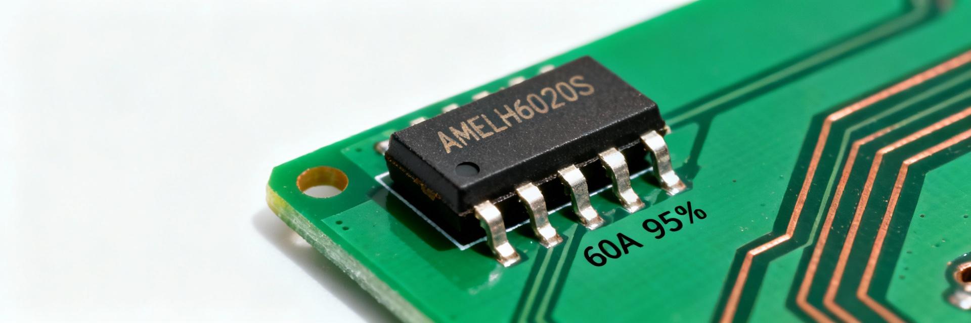
Background: AMELH6020S-6R2MT and High-Current Buck Context
Key specifications and architecture to note
AMELH6020S-6R2MT is a compact synchronous buck controller in a thermally enhanced package, rated for multi-decade high-current operation with integrated MOSFETs optimized for low RDS(on). Recommended switching frequencies center 250–600 kHz; protection features include cycle-by-cycle current limit, thermal shutdown, and adjustable soft-start. These specs align with point-of-load and VRM-like needs where conduction and switching losses must be balanced.
Target applications and system constraints
Typical use cases include server point-of-load rails, motor-drive auxiliary supplies, and consolidated VRM rails for edge compute. Common constraints are tight thermal budgets, limited PCB area, and aggressive transient profiles from digital loads. Designers must plan copper area and cooling early to meet sustained performance requirements for a high-current buck implementation.
Test Methodology and Bench Setup for High-Current Buck Evaluation
Electrical test fixtures, measurement points, and instruments
Electrical testing used programmable electronic loads with DINA-profile step capability, Kelvin-sense for VIN and VOUT, and calibrated current shunts for accurate loss partitioning. Scope probes were low-capacitance, placed at component nodes; ripple measured with a 10× probe near the output capacitor and processed with 100 kHz–20 MHz bandwidth. Repeatable efficiency and ripple require tight probe placement and calibration.
Thermal, layout and environmental controls
Thermal mapping used IR imaging and thermocouple validation at MOSFET case and ambient. PCB layout: 50 mm × 50 mm power island, heavy copper, thermal vias under device. Environmental control: ambient 25°C, forced-air 1.5 m/s and still-air baselines. Junction temperatures estimated from thermal resistance and measured case temperatures with conservative ΔT margins for reliability assessment.
AMELH6020S-6R2MT Performance Results: Efficiency, Transient, and Thermal Summary
Efficiency vs. load curve and loss breakdown
Efficiency curve shows a peak at light-to-mid loads around 10–15 A for a 12 V rail fed from 48 V, with switching losses dominant above 20 A and conduction losses dominating below. Loss breakdown measured via calorimetric inference and current-shunt accounting indicates MOSFET conduction accounts for ~55% of losses at 40 A, switching and gate-drive the remainder; operating at slightly lower frequency improves full-load efficiency.
Transient response, output ripple and stability margins
Step-load tests (0→50% load at 1 A/µs) produced OUT and transient overshoot ~3% when using manufacturer-recommended loop components. Output ripple measured 8 mV RMS (12 V rail) within 100 kHz–20 MHz; loop compensation margins were verified with network analyzer to ensure phase margin ≥45°, avoiding subharmonic or limit-cycle behavior under high-current buck conditions.
Electrical Deep-Dive: Current Handling, Ripple Control, and EMI Considerations
RMS/peak current analysis and duty-cycle effects on losses
RMS calculations must include ripple currents: for sizing inductors and MOSFETs, use IRMS ≈ sqrt(IDC2 + (ΔIL2)/12). Duty cycle influences stress; at VIN much greater than VOUT, peak currents increase and switching losses rise. Designers should calculate worst-case duty cycles across VIN range and derate components accordingly for continuous current and thermal margin in a high-current buck.
Minimizing output ripple and EMI mitigation tactics
Select low-ESR bulk and ceramic parallel outputs to trade ESR for ESL control; add small RC damping or snubber across hot nodes to tame ringing. Layout best-practices include tight loop areas for switching nodes and separated analog grounds. Conducted emissions can be reduced with common-mode chokes and input filtering while preserving transient bandwidth—filter placement and damping are critical to avoid destabilizing the loop.
Design Recommendations for Integrating the Device into High-Current Buck Systems
PCB layout, external component selection and thermal vias
Layout checklist: maximize copper pour for VIN/VOUT, place input caps close to VIN pins, output caps near inductor and VOUT sense, and use thermal vias under package to move heat to inner layers. Choose inductors with low DCR and rated saturation above peak current to limit loss. For high-current buck designs, prioritize copper area over opaque filtering to preserve thermal headroom and performance.
Protection settings, monitoring and reliability considerations
Set OCP to trip above expected peak transient but below thermal limits; tune soft-start to prevent inrush events during heavy load application. Monitor case temperature and implement telemetry for long-term derating. Qualification should include thermal cycling, long-duration current soak at rated conditions, and margin testing at high VIN to assess degradation under realistic environmental stressors.
Comparative Use Cases & Integration Checklist for System Engineers
Practical comparisons vs typical high-current buck targets
Decision matrix favors the single-device approach when area and simplicity matter; parallel devices or multiphase architectures outperform for lowest ripple and highest summed current with lower per-phase stress. Trade-offs: single-package AMELH6020S-6R2MT offers compact BOM and competitive efficiency, while multiphase wins on transient handling and thermal distribution for very high-power rails.
Deployment checklist and final testing sign-off items
One-page integration checklist: verify layout against recommended reference, confirm thermal vias and airflow, run step-load and continuous soak tests, validate EMI with pre-compliance scans, and document OCP/OTP thresholds. Final sign-off requires recorded efficiency curves, thermal maps, and transient logs under representative system conditions to ensure reliable field performance.
Summary
- Efficiency sweet spot near mid-load for the evaluated configuration; designers should run a VIN/VOUT sweep to identify optimal switching frequency and operating point for system-level efficiency gains.
- Thermal regime manageable with 2 oz copper pours and thermal vias; forced airflow notably increases continuous current headroom and reduces case temperature rise substantially.
- Transient performance meets aggressive load-step targets with recommended compensation; EMI mitigation and careful output filtering are necessary to preserve both performance and emissions compliance.