News Center
Understand customer needs and strive for excellence in quality, delivery, service, and environmental responsibility
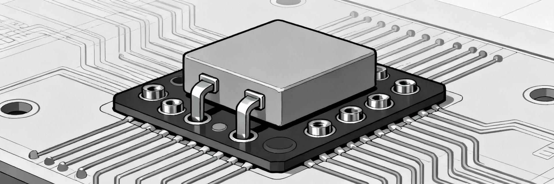
AMELH6030S-4R7MT: Optimize PCB Layout for SMD Inductors
Date:
2026-02-03 11:17:13
Source:
Browse:
0
Practical PCB layout rules to minimize heating, reduce EMI, and preserve inductance under DC bias for high-performance power converters.
Why the AMELH6030S-4R7MT Matters for Power Design
Electrical & Mechanical Specs
Confirming component datasheet values is critical. The AMELH6030S-4R7MT features a nominal inductance of 4.7 µH with a package footprint of approximately 6.8 × 6.6 × 3.1 mm. DCR drives steady-state heating, while Isat sets derating margins.
SMD Inductor Behavior
Magnetic coupling and proximity effects change effective inductance. Placement should preserve the intended core flux path and avoid nearby return-path disruptions that amplify EMI and decrease effective inductance under load.
Thermal and Current-Related Considerations
Saturation Margin Visualization (Example: 15A Rated)
*Recommended 20-30% derating margin to avoid core saturation.
Thermal Path Design
Spread heat from the inductor into internal planes using a copper pour on adjacent layers. Stitch the exposed pads with an array of 6–12 plated thermal vias (0.3–0.5 mm drill) in a staggered pattern for maximum heat dissipation.
DC Bias Validation
Validate in-circuit by measuring effective inductance with a low-frequency LCR meter or by probing the switching node under controlled DC bias. Ensure expected peak current stays below the derated threshold.
Best Practices for Placement and Routing
| Category |
Key Requirement |
Optimization Logic |
| Placement |
Adjacent to switching node & caps. |
Minimizes distance to critical caps, reducing loop area and conduction loss. |
| Routing |
Short, wide traces; uninterrupted GND. |
Lowers radiated EMI and ringing; prevents noise coupling into sensitive nodes. |
| Footprint |
60–80% solder paste coverage. |
Prevents part tilting and ensures consistent fillets for reliable joints. |
Case Study: Synchronous Buck Converter Layout
Placement Sequence
- Switching FETs: Fix the switch-node reference.
- Inductor: Place adjacent to FETs and output caps.
- Input/Output Caps: Decouple VIN and finalize the output loop.
- Control Logic: Keep sensitive traces away from the inductor.
Validation Metrics
- ✅ Reduced ΔT at inductor (several °C)
- ✅ EMI peak reduction (3-6 dB)
- ✅ Minimized switch-node overshoot
- ✅ Higher efficiency at peak loads
Pre-Production Checklist
PCB Review Items
- Verify pad dimensions match mechanical outline
- Count thermal vias (Target: 6–12)
- Check copper pour clearances
- Confirm return path continuity
Lab Validation
- Thermal imaging under full load
- In-circuit DC-bias check
- Oscilloscope probing for ringing
- Conducted/Radiated EMI scans
Summary
- Verify key datasheet values (4.7 µH nominal) and derate the AMELH6030S-4R7MT for DC bias and saturation; ensure pad and height keepouts match the mechanical outline.
- Prioritize thermal copper and via stitching beneath and around the inductor to spread heat; use multiple small vias (0.3–0.5 mm drill) tied to internal planes to reduce temperature rise.
- Minimize switching loop area with the shortest, widest traces and an uninterrupted return plane to reduce EMI and preserve inductance.
Frequently Asked Questions
How should I verify AMELH6030S-4R7MT derating for my PCB layout?
+
Measure the expected peak DC current in your topology and apply a conservative derating—commonly 20–30% below the datasheet Isat. Validate on the board by measuring inductance under DC bias or by running the converter at worst-case load while monitoring core temperature and switching waveforms for signs of saturation.
How many thermal vias should be placed under the inductor pad?
+
Use a distributed array—typically 6–12 plated vias (drill ~0.3–0.5 mm) beneath or around the thermal land—to connect to internal copper planes. Space them in a staggered grid to maximize thermal coupling and coordinate with your PCB fabricator for via paste and tenting rules.
Will more solder on the pads improve thermal performance?
+
Not necessarily. Excessive solder increases fillet size and can tilt the part, changing stray coupling and possibly degrading EMI or inductance. Aim for controlled paste coverage (around 60–80%), verify the reflow profile, and inspect fillets for consistency to balance thermal contact and electrical performance.