
Engineers validating power converters and automotive-grade designs require a focused, data-driven approach to component selection. This article provides a technical, component-level deep dive for the HCM1A1307V3 with practical datasheet analysis and measurement steps to determine suitability for high-current buck converters and harsh-environment use. It frames which datasheet fields to extract, how to read L(f) and impedance curves, how to quantify losses and temperature rise, and how to apply derating and transient limits. The goal is to let a design engineer move from datasheet to validated board-level behavior using specific formulas, example calculations, and verification procedures that fit production validation workflows.
All guidance references the component’s published datasheet fields generically (inductance variants, DCR, Isat, rated current, temperature limits, mechanical footprint) and shows where to extract values for practical checks. Use the checklists and example sizing calculations below to convert datasheet numbers into conservative electrical limits and test plans for production validation.
1 — Product & Datasheet Overview (background)
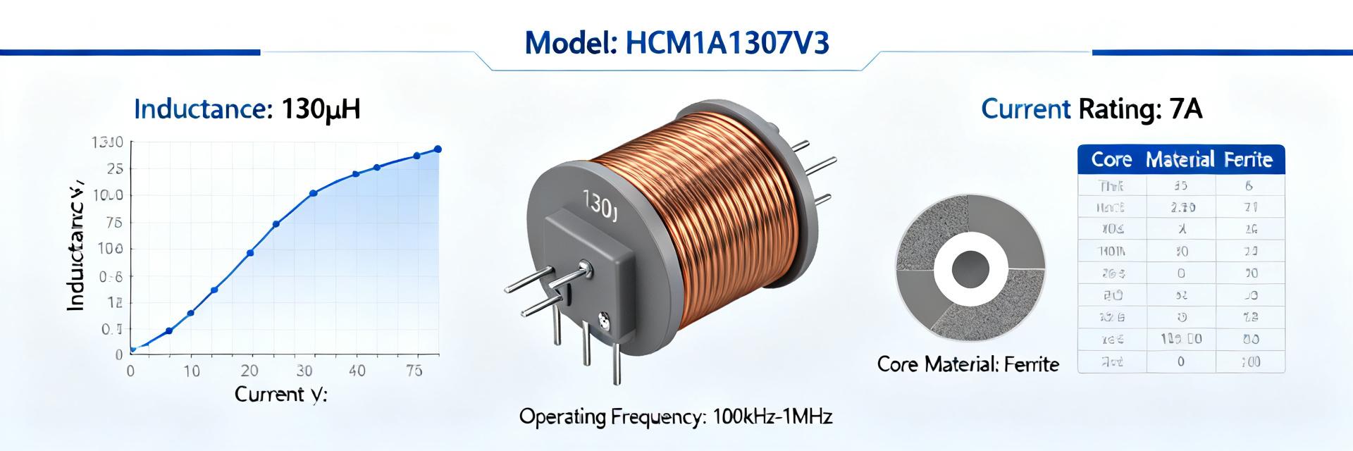
Key specifications at a glance
Point: Start by extracting explicit fields: inductance variants (e.g., 4R7 / 1R0 ranges), typical & max DCR, rated DC current (Irated), saturation current (Isat defined as X% inductance drop), operating temperature range, maximum ambient/board temperature, mechanical dimensions, and packaging. Evidence: These entries are commonly tabulated under “electrical characteristics” and “mechanical data” in the component’s datasheet. Explanation: Record typical vs maximum DCR, Irated (continuous), and Isat (often specified at a given ΔL%); note tolerance and units and flag ambiguous table entries for vendor confirmation during procurement.
Mechanical & thermal notes
Point: Mechanical footprint and thermal conduction dictate board-level thermal rise and assembly risk. Evidence: Datasheet mechanical drawings show pad pattern, recommended solder fillet, component height and gross mass. Explanation: Confirm pad geometry matches PCB footprint, check recommended solder profile and maximum reflow temperature, and plan thermal vias or copper pours to lower junction-to-ambient thermal resistance; watch for warpage risk on large pads and solder fillet control that affect mechanical reliability.
| Parameter | Typical Datasheet Value | What to check | Example note |
|---|---|---|---|
| Inductance variants | 4R7 / 1R0 / 220 | Nominal value & tolerance | 4R7 = 4.7 μH; confirm tolerance ±20% |
| DCR (typ / max) | 10 mΩ / 15 mΩ | Measure at 25°C, check max for heating | Use max DCR for loss estimate |
| Rated DC current (Irated) | e.g., 10 A | Continuous rating and test conditions | Derate for ambient & PCB temp |
| Saturation current (Isat) | e.g., 20 A (@30% ΔL) | Definition of ΔL and test freq | Use for peak current checks |
2 — Electrical Characteristics & Frequency Behavior (data analysis)
Impedance, inductance vs frequency, and resonance
Point: Read impedance vs frequency and L(f) plots to identify SRF and usable band. Evidence: Datasheet curves show L(f) falling with frequency and an SRF peak where inductive behavior gives way to capacitive. Explanation: Select the operating band below SRF and extract L at switching frequency accounting for DC bias and tolerance. Example: for fs = 500 kHz, read L at 500 kHz or interpolate; calculate ripple current ΔI = (Vin - Vout) * D / (L * fs) for a buck (D = Vout/Vin). If Vin=12 V, Vout=5 V, L=4.7 μH, fs=500 kHz: D≈0.4167 → ΔI ≈ 1.24 A (useful to size Isat and thermal loss).
Loss mechanisms and efficiency impact
Point: Separate I²R (DCR) losses from core/AC losses. Evidence: Datasheet gives DCR; core loss is expressed in separate curves vs frequency and flux (or approximate vendor loss tables). Explanation: Compute DC loss P_DCR = I_rms² × DCR (I_rms ≈ sqrt(Iout² + ΔI²/12) for triangular ripple). Estimate core loss from published L(f)-bias or core-loss curves at the operating flux density—if not available, use a conservative multiplier. Sum losses to predict steady-state temperature rise via thermal resistance (θJA) or board-level empirical ΔT per watt.
3 — Electrical Limits, Derating & Reliability (method guide)
DC rating, saturation, and derating rules
Point: Treat Irated as a continuous guideline and Isat as a peak/limit defined by ΔL% (often 10–30%). Evidence: Datasheet fields labeled “Rated current” and “Saturation current (Isat)” must include test conditions (temp, %L drop, test frequency). Explanation: Design continuous current at 60–80% of Irated depending on airflow and ambient; ensure peak (Ipk = Iout + ΔI/2) stays below Isat where inductance reduction is acceptable. List exact datasheet fields to check: Irated, Isat (definition), DCR (typ/max), temperature range and thermal derating curves.
Transient currents, inrush, and reliability limits
Point: Transients can exceed Isat briefly but cause stress. Evidence: Some datasheets list surge or pulse current limits; if absent, use thermal time constants and solder fatigue considerations. Explanation: Model startup/inrush as short pulses—compare energy (∫I²dt) to component thermal capacity; evaluate cumulative stress from thermal cycling, vibration, and solder fatigue. If the datasheet lacks vibration or thermal cycle data, apply larger derating margins or select a variant with higher Isat and lower DCR.
4 — Measurement & Verification Procedures (case / practical testing)
Recommended bench tests and setups
Point: Verify datasheet claims with controlled bench tests: L(f), impedance, DCR, and thermal under load. Evidence: Use an LCR meter for low-frequency L and DCR, a VNA for impedance vs frequency, and a programmable electronic load or waveform generator plus DC supply for pulsed/current-stress tests. Explanation: Use short, low-parasitic fixtures, calibrate for fixture inductance, run current pulses while monitoring temperature with thermal imaging. For EMI checks, perform near-field scans around the inductor and switching node.
Interpreting discrepancies and corrective actions
Point: Measurement differences often come from fixtures, DC bias, or temperature. Evidence: Observed lower L under DC bias or higher DCR at elevated temperature is expected. Explanation: Compensate by subtracting fixture parasitics, repeat measurements at expected board temperature, and if results deviate, apply fixes: enlarge copper for cooling, add thermal vias, parallel inductors, or choose a higher-current variant with higher Isat.
5 — Design Integration Checklist & Sizing Examples (action)
PCB layout and thermal-management checklist
Point: Layout controls heating and ESR path integrity. Evidence: Datasheet pad patterns and thermal notes indicate recommended via counts and land patterns. Explanation: Place the inductor close to the switching device, route high-current traces with wide copper and multiple vias, implement thermal vias under adjacent copper pours, keep sensitive analog return paths away, and follow solder reflow profiles to avoid mechanical stress.
Sizing example and margin calculations
Point: Example to select variant for a buck: Vin=12 V, Vout=5 V, Iout=10 A, fs=500 kHz. Evidence: Use ΔI formula and DCR loss template above. Explanation: For L=4.7 μH, ΔI ≈ 1.24 A → Ipk ≈ 10 + 0.62 = 10.62 A. Check Isat > Ipk with margin and DCR (use max DCR) to compute P_DCR. Compute I_rms ≈ sqrt(10² + 1.24²/12) ≈ 10.02 A; if DCR=10 mΩ → P_DCR ≈ 1.0 W. Apply 60–80% derating on Irated for continuous operation in limited airflow and re-evaluate; if Isat or thermal margin insufficient, choose a higher-current variant or parallel inductors per decision tree.
Summary
This analysis shows how to convert datasheet fields into actionable design decisions for the HCM1A1307V3: extract inductance variants, DCR (typ/max), Irated and Isat definitions, and mechanical/thermal notes to build a verification plan. Use impedance and L(f) curves to pick the operating band below SRF, calculate ripple current and losses with the provided formulas, and apply conservative derating (60–80%) for continuous duty in harsh environments.
- Extract and record key datasheet fields (inductance, DCR, Irated, Isat, temperature range) and confirm test conditions before acceptance—this datasheet analysis step prevents mis-sizing during validation.
- Use L(f) and impedance curves to determine usable inductance at switching frequency and compute ΔI = (Vin−Vout)·D/(L·fs); check Ipk vs Isat and compute P_DCR = I_rms²·DCR for thermal budgeting.
- Apply derating: design continuous current at 60–80% of Irated depending on board cooling; verify with bench tests (LCR/VNA, pulsed current, thermal imaging) to confirm electrical limits and long-term reliability.


