AMELH6060S-R47MT Datasheet: Read Specs & PCB Footprint
PCB designers and power engineers often waste prototype cycles chasing inductors whose specifications or footprint don’t match the intended layout — costing time and budget. This guide cuts through that friction by showing exactly where to verify the AMELH6060S-R47MT datasheet, how to interpret key specs, and how to implement a reliable PCB footprint to avoid re-spins and unexpected thermal or EMI problems.
For pragmatic verification, treat the manufacturer product page and authorized-distributor PDFs as primary evidence sources and always confirm datasheet revision and test conditions before finalizing BOM fields. This article highlights electrical specs and PCB footprint actions, plus thermal and assembly safeguards you can apply immediately.
1 — Product overview & where to get the AMELH6060S-R47MT datasheet (Background)
1.1 Datasheet sources & revision check
Point: Obtain the official part datasheet from the OEM product page or an authorized distributor PDF and confirm revision IDs. Evidence: the datasheet header typically lists a revision code and a “DOCUMENT CHANGE” or date stamp. Explanation: when you search for the AMELH6060S-R47MT datasheet PDF download, record the revision and compare electrical tables — small changes in Isat, DCR, or recommended land pattern can affect final selection and assembly.
1.2 Key product ID & short spec snapshot
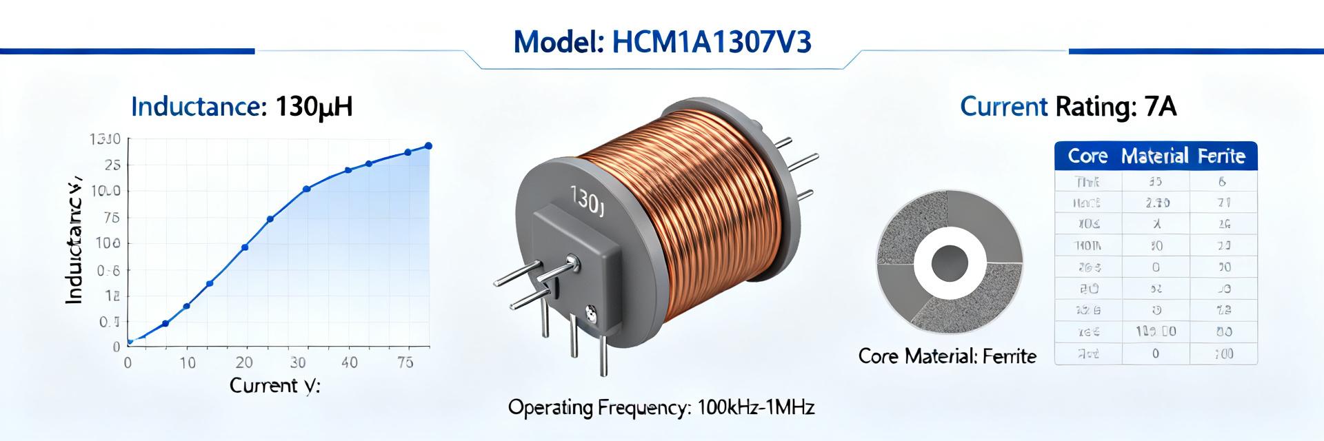
Point: Identify the one-line product description and primary electrical markers. Evidence: this part is a molded power inductor, nominal inductance 0.47 µH, part marking codes, and a max operating temperature range commonly around -40°C to +125°C. Explanation: knowing the basic ID, inductance, and temperature range quickly filters candidates for switching regulators and establishes expected derating behavior under continuous load.
2 — Electrical specs deep-dive: inductance, current, SRF, and losses (Data analysis)
2.1 Inductance, tolerance, and DC resistance (DCR)
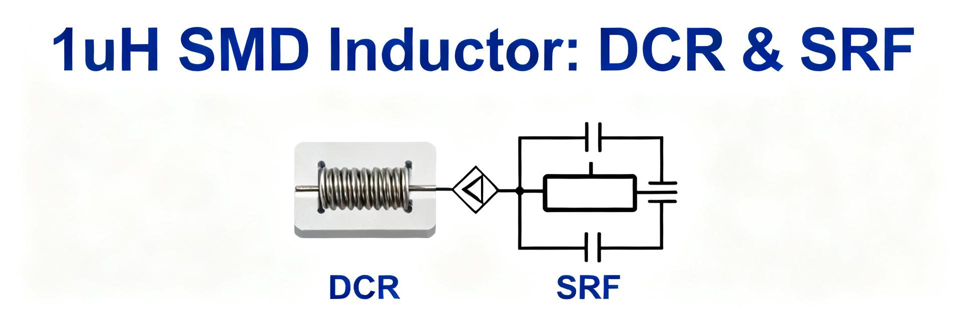
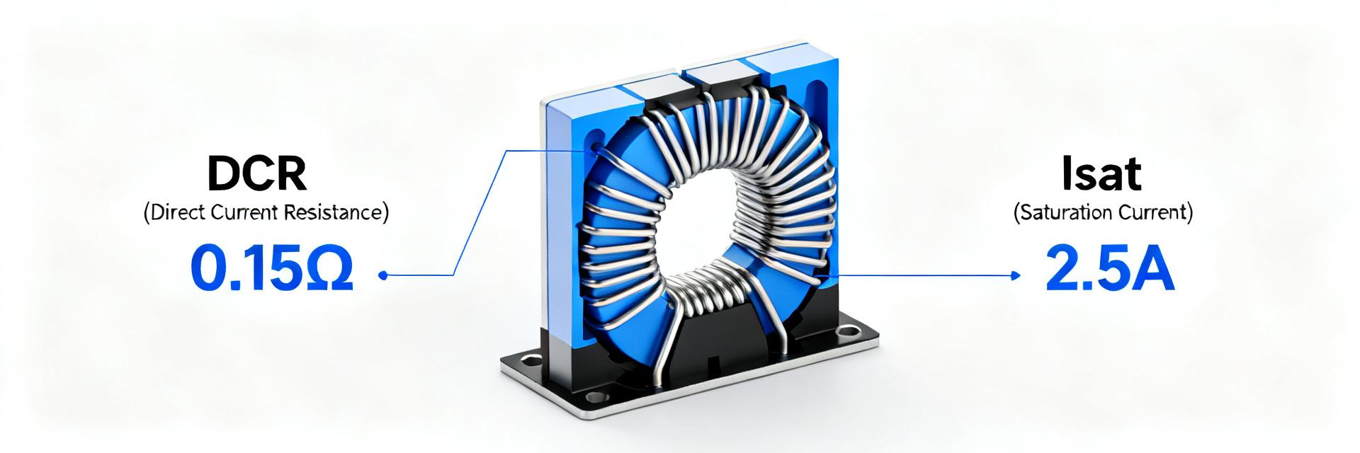
Point: Read the inductance value, tolerance, and listed DCR carefully; these specs drive loss and efficiency. Evidence: the datasheet shows inductance at 100 kHz/0.1 Vrms and lists DCR in milliohms under specified temperature. Explanation: when comparing specs, use the listed measurement frequency and method; DCR impacts conduction loss (I²R) so pick parts with minimal DCR consistent with acceptable Isat and thermal rise during steady-state operation.
2.2 Rated current, saturation characteristics, and SRF
Point: Use Isat and Irms tables plus any saturation curves to size margin for peak currents. Evidence: datasheets provide Isat defined at a specific inductance drop (e.g., 25%) and often include SRF values identifying where the inductor becomes reactive. Explanation: select parts with Irms above expected continuous current and Isat comfortably above expected peaks; ensure switching frequency is well below SRF to avoid degraded inductance and EMI consequences.
3 — Mechanical dimensions & recommended PCB footprint (Method guide)
3.1 Dimensional drawing interpretation
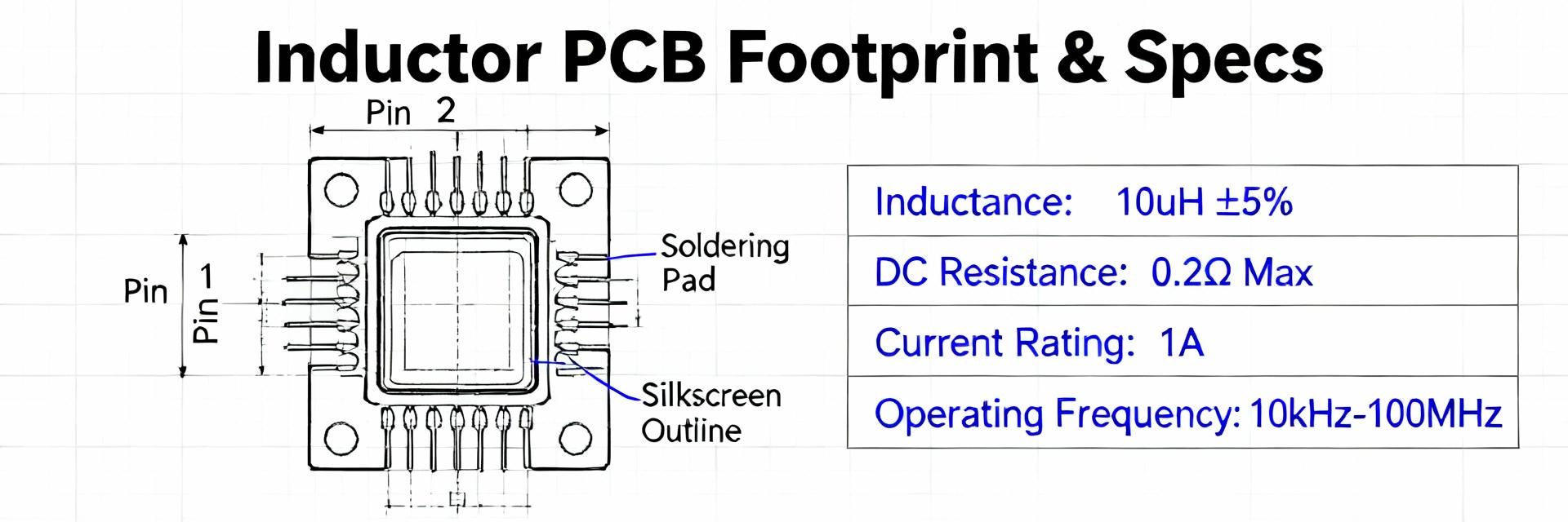
Point: Extract L×W×H, pad geometry, and tolerance callouts from the mechanical drawing. Evidence: the drawing lists nominal dimensions (for 6060 package, typical lengths around 6.0 mm) and pad-to-pad spacing with tolerance bands. Explanation: translate those dimensions to footprint pads with proper fillet expectations and note keepout zones for adjacent components to prevent solder wicking and mechanical interference during reflow.
3.2 Recommended land pattern + Gerber export tips
Point: Create a land pattern using the datasheet pad recommendations and export Gerbers with clear solder mask and paste definitions. Evidence: recommended pad sizes and paste aperture percentages are given; use a slightly reduced paste aperture for large pads to avoid tombstoning. Explanation: an AMELH6060S-R47MT PCB footprint recommended land pattern typically uses rectangular pads sized to the datasheet, solder mask openings per pad, and a 60–80% paste aperture to control joint fillet; name footprint files clearly for CAD libraries (example: AMELH6060S-R47MT_LP.kicad_mod).
4 — Thermal, assembly, and reliability considerations (Method / Data)
4.1 Thermal performance & derating guidelines
Point: Apply derating curves to continuous current ratings and assess board temperature rise. Evidence: datasheet thermal cues such as allowable ambient and temperature rise at specified current give practical limits. Explanation: derate continuous current by 10–30% depending on board cooling; place the inductor away from heat sources and provide copper pour or thermal vias if needed to lower junction rise during sustained loads.
4.2 Soldering profile, reflow compatibility, and placement rules
Point: Follow recommended reflow temperature curves and placement orientation to avoid mechanical damage. Evidence: reflow max peak temperatures and recommended time-above-liquidus are listed in assembly notes. Explanation: use manufacturer-recommended profiles, avoid excessive hand-solder heating, verify placement with test pick-and-place runs, and consider IR thermal imaging and power cycling to validate reliability after assembly.
5 — Selection, procurement, and close equivalents (Case study + Action)
5.1 BOM & procurement checklist
Point: Populate BOM fields with full part number, tolerance, packaging, and datasheet revision. Evidence: missing tape/reel or revision info often causes wrong buys. Explanation: include full part code, inductance tolerance, packaging option, MOQ, and the verified datasheet revision on the BOM; use authorized-channel procurement and require traceability to reduce counterfeit risk.
5.2 Cross-references and substitution strategy
Point: When substituting, match inductance, Isat, DCR, SRF, and footprint before qualification. Evidence: small differences in SRF or DCR can alter regulator loop behavior. Explanation: accept substitutions only after confirming electrical specs and mechanical fit; re-run thermal and EMI checks for any cross-referenced part to avoid surprises in the final assembly.
Summary
- Verify the AMELH6060S-R47MT datasheet revision before finalizing the BOM; confirm inductance, DCR, Isat/Irms and measurement conditions to ensure the part meets electrical specs and reliability targets.
- Translate the mechanical drawing into an AMELH6060S-R47MT PCB land pattern using datasheet pad sizes, paste aperture guidance, and solder mask clearances to avoid re-spins.
- Apply thermal derating and follow recommended reflow profiles, placement rules, and verification testing (IR imaging, power cycling) to ensure assembly reliability and reduce field failures.
Frequently Asked Questions
What key items should I check first in the AMELH6060S-R47MT datasheet?
Check the nominal inductance and tolerance, DCR at specified temperature, rated Irms and Isat definitions, SRF, and mechanical land pattern dimensions. Confirm the datasheet revision and test conditions; mismatches in measurement frequency or revision numbers are common root causes of poor field performance.
How do I ensure my PCB footprint matches the AMELH6060S-R47MT?
Extract pad geometry and tolerances from the mechanical drawing, set paste apertures to 60–80% for large pads, define solder mask clearance per recommendation, and export Gerbers with distinct layer names. Validate the footprint with a 1:1 print and placement test before full production.
When should I worry about SRF and switching frequency for the AMELH6060S-R47MT?
If your switching frequency approaches a significant fraction of the SRF, inductance will fall and EMI behavior will change. Choose an inductor with SRF comfortably above the switching band or run impedance measurements to confirm acceptable inductance at operating frequency and to avoid filter resonance issues.