AMELH6020S-R82MT Datasheet Deep Dive: 820nH, 17A Specs
Designed for high-current power rails, the AMELH6020S-R82MT delivers 820 nH inductance with rated current capability up to 17A — parameters that directly affect switching loss, ripple current, and thermal budget in modern DC–DC converters. This deep dive gives a practical interpretation of datasheet numbers, a bench-validation recipe for inductor performance, and concrete PCB integration rules so engineers can decide quickly whether this 820nH, 17A SMD inductor fits their design.
This article focuses on what to capture from the datasheet, how to estimate I2R loss and temperature rise, and step-by-step layout and EMI mitigations to validate the part in a real converter. Expect concise calculations, a bench checklist, and a selection decision matrix you can apply on the lab bench and in CAD.
1 — Background & where this part fits (background introduction)

1.1 Key electrical specs at a glance
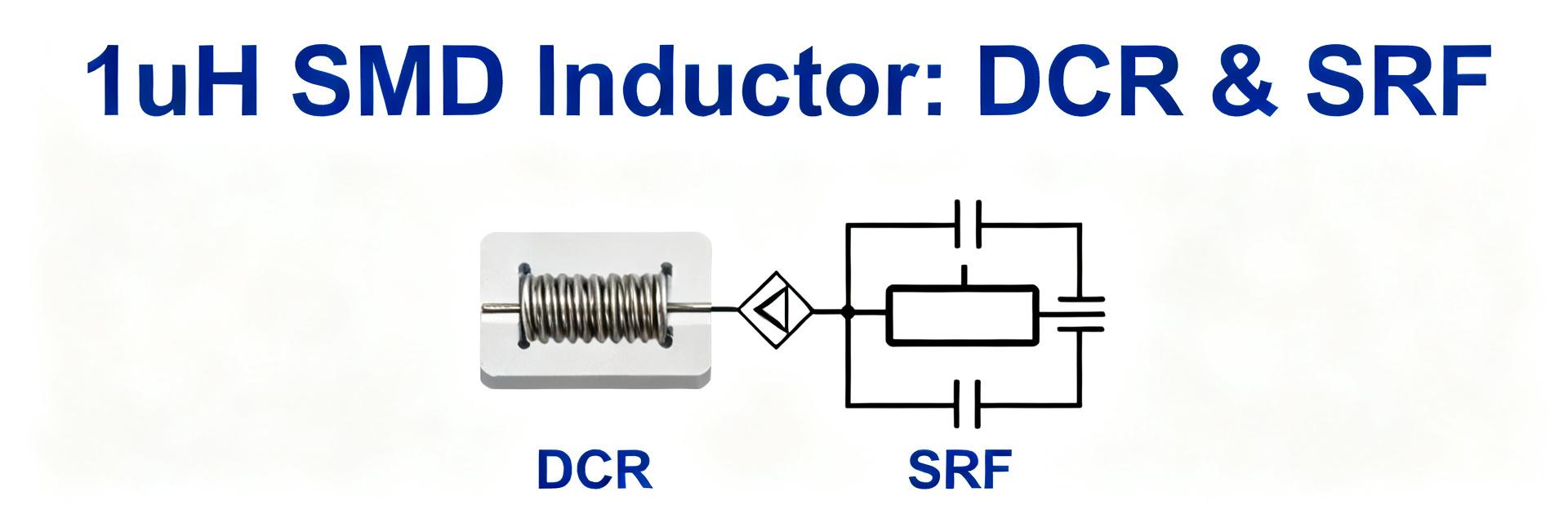
Point: Extract headline specs first — nominal inductance, rated current, DCR, Isat/Irms definitions, operating temperature, and mechanical dimensions. Evidence: Typical datasheet entries show nominal inductance 820 nH, rated current 17A, and a DCR specified as typical/max. Explanation: Designers use 820nH to set ripple and loop dynamics; DCR determines I2R conduction loss and thermal budget; Isat/Irms dictate usable current range under DC bias and heating.
1.2 Mechanical footprint & board-level constraints
Point: Record package footprint, SMD mounting style, land pattern and height before library creation. Evidence: Datasheet mechanical drawings list pad recommendations, overall height and recommended solder fillet. Explanation: Copy land pattern, recommended pad shape, and height into your PCB library; observe height limits for enclosures and keep the part away from heat sources to prevent thermal derating during high-current operation.
2 — Electrical performance deep-dive (data analysis)
2.1 Inductance vs frequency and DC bias (Isat/Irms interpretation)
Point: Read L vs frequency and L vs DC bias curves to predict behavior under switching and DC load. Evidence: Datasheet L(f) shows small decrease with frequency; L(I) shows drop as DC current grows toward Isat. Explanation: Define Isat as the DC current at which L drops ~30% and Irms as the current that produces the specified temperature rise; the 17A rating is a design-point where you must confirm whether it refers to Isat or Irms and size your margin accordingly to avoid unacceptable inductance loss in the converter loop.
2.2 DCR, Q-factor, and saturation behavior
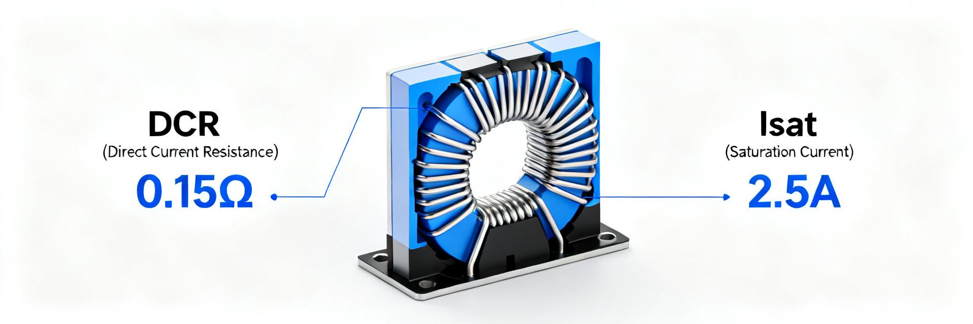
Point: Quantify conduction loss and frequency behavior via DCR and Q-factor. Evidence: Use P = I^2 × DCR for steady-state loss; Q = (ωL)/RAC from impedance data for resonance and EMI insights. Explanation: If DCR = 10 mΩ (example), P at 17A = 17^2×0.01 = 2.89 W — a thermal-design driver. Summarize saturation as soft (gradual L drop) or hard (abrupt) from the manufacturer curves to anticipate converter transient responses.
| Example parameter | Value (example) | Use |
|---|---|---|
| DCR (typ) | 0.010 Ω | I2R loss calc: P = I^2×DCR |
| Inductance | 820 nH | Set ripple: ΔI = V×D/(L×fS) |
3 — Thermal, reliability & derating (method/guideline)
3.1 Temperature rise, thermal resistance, and power loss budgeting
Point: Estimate temperature rise from measured power loss and board thermal path. Evidence: Compute power loss P = I^2 × DCR (use operating current or Irms) and convert to ΔT via thermal resistance θ (junction-to-ambient). Explanation: Step 1 — calculate P; Step 2 — measure or estimate θboard (°C/W) including copper pours and vias; Step 3 — ΔT = P×θ; Step 4 — ensure ambient + ΔT remains below max operating temperature and keep a safety margin (typically 20–30%). Log max operating temp, storage temp, and MSL if present for reliability tracking.
3.2 Long-term reliability & environmental considerations
Point: Account for mechanical and environmental stress on SMD inductors. Evidence: Thermal cycling, humidity, and vibration degrade solder and core materials over time. Explanation: Check datasheet for MSL and compliance notes; run qualification tests — thermal cycling, solderability and high-temperature soak — focusing on solder fillet integrity and inductance drift. Plan cycles and acceptance criteria matching your product life expectations.
4 — PCB integration & EMI best practices (method/guideline + case)
4.1 Layout and footprint best practices for 820nH, 17A applications
Point: Optimize copper and vias to carry 17A with low series resistance and good thermal conduction. Evidence: Use wide traces or copper pours, multiple thermal vias under the pad, and minimize series loop area. Explanation: For continuous 17A, prefer heavy copper (2 oz) or parallel pours and a trace width sufficient to keep temperature rise acceptable; ensure recommended pad sizing and fillet for reliable solder joints and reduced thermal resistance to the board.
4.2 Magnetic coupling, shielding, and EMI mitigation
Point: Reduce radiated and conducted EMI by controlling placement and coupling. Evidence: Place the inductor away from sensitive analog nets and orient to minimize loop coupling; use ground plane partitioning and shielded vias where needed. Explanation: Run impedance sweeps and near-field probe checks to locate hot spots; keep switching node loops tight, and use common-mode filtering if conducted emissions persist. Document test set-up and baseline EMI measurements before layout changes.
5 — Validation checklist & selection decision matrix (action suggestions)
5.1 Bench test checklist to validate 820nH at target current
Point: Follow a reproducible bench sequence to validate inductance and losses under load. Evidence: Measure L with LCR meter at DC bias, measure DCR with 4-wire, perform thermal-rise test at planned operating current, and test in-circuit under switching load with scope. Explanation: Record ambient temp, fixture details, meter model, and probe placement. Report L vs I, DCR vs temperature, and thermal images or logged ΔT to verify that actual behavior matches datasheet claims.
5.2 When to choose this part — selection criteria & alternatives to consider
Point: Use a decision matrix comparing DCR, Isat/Irms margin, height/footprint, thermal performance and cost. Evidence: If low DCR, compact size and a ≥ target-current margin are priorities, this family is attractive; otherwise consider alternatives with lower height or higher inductance. Explanation: Rank candidates by required margin (e.g., target current ≤ 80% Irms), DCR-driven power loss, PCB area, and mechanical constraints, then prototype the top choice to confirm thermal and EMI behavior.
Key summary
- Confirm nominal inductance and DC-bias behavior: measure L vs I to ensure the 820 nH value remains acceptable under converter DC bias and switching conditions.
- Compute conduction loss from DCR: use P = I^2 × DCR with operating current to estimate thermal load and design copper/vias for heat removal.
- Follow layout rules for 17A: use heavy copper or parallel pours, thermal vias under pads, and minimize loop area to reduce I2R loss and EMI.
- Validate on bench: LCR with DC bias, 4-wire DCR, thermal-rise at operating current, and in-circuit switching tests are required before production.
Common questions
What bench tests confirm the inductor meets its specified inductance and current rating?
Measure inductance with an LCR meter while applying representative DC bias (L vs I sweep), measure DCR with a 4-wire method, then run a thermal-rise test at target current. In-circuit switching tests with scope capture ripple and transient saturation behavior; report ambient temperature and fixture details for repeatability.
How do you compute power loss for a 17A design using DCR?
Use P = I^2 × DCR. For continuous current, use the expected RMS current; include switching ripple when it significantly increases RMS. Translate P into ΔT using measured or estimated board thermal resistance to verify the part stays within rated temperature limits.
What layout changes reduce EMI when using a high-current 820nH inductor?
Minimize switching loop area, place the inductor close to its associated capacitor and switch node, use solid ground planes, add thermal vias, and keep sensitive analog traces distant. Validate with near-field probes and conducted emission sweeps and iterate based on measured hotspots.
In summary, the AMELH6020S-R82MT provides 820 nH inductance with design-grade current capability (17A); validate inductance under DC bias, compute I2R losses from DCR, and apply robust PCB thermal and EMI practices before committing to production.