2.2uH Power Inductor Soldering & Mounting Guide & Tips
Many engineers and technicians see overheating, poor reflow yields, or mechanical failures when mounting a 2.2uH power inductor; this concise soldering guide fixes that with practical, tested steps. This article focuses on selection, PCB footprint, reflow and hand-solder workflows, common failure modes and fixes, and mounting tips to improve thermal and mechanical reliability in production and repair.
The recommendations reflect hands-on assembly experience and measurement checks (DCR, Isat, thermal imaging). Expect clear selection checklists, specific land-pattern guidance, reflow profile notes, and conservative hand-solder procedures suitable for US production environments. The model AMELH6030S-2R2MT is used as an example geometry reference only; avoid assuming all parts share identical limits.
Component selection: choosing the right 2.2uH power inductor

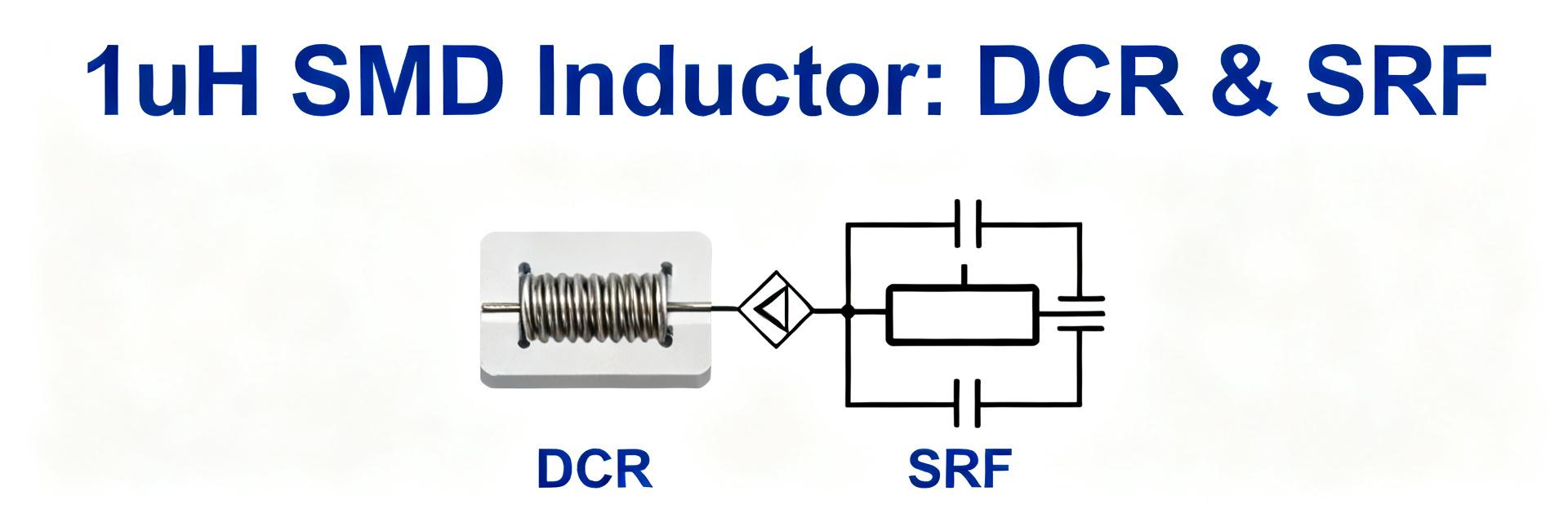
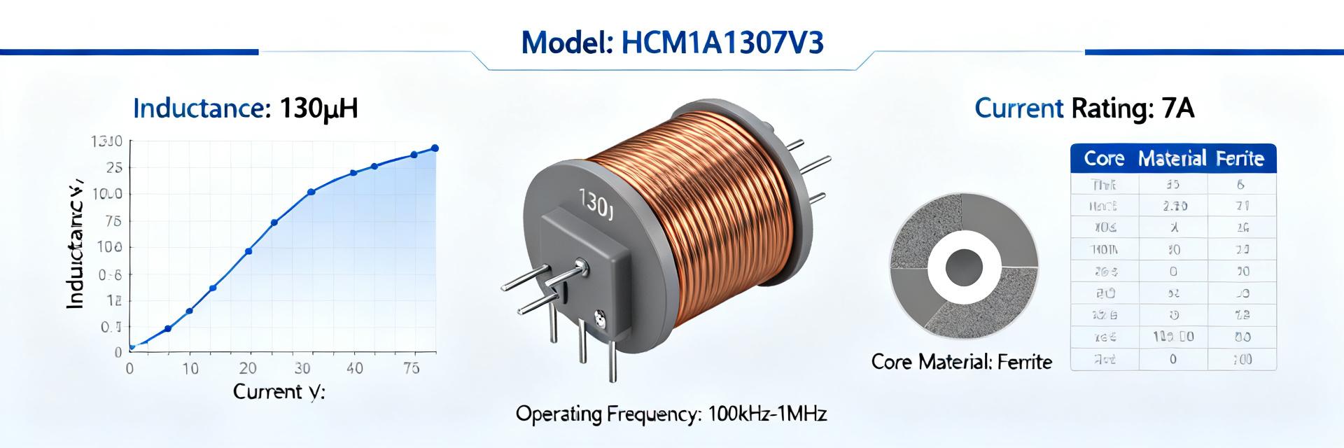
Key electrical specs to compare (current rating, DCR, Isat, SRF)
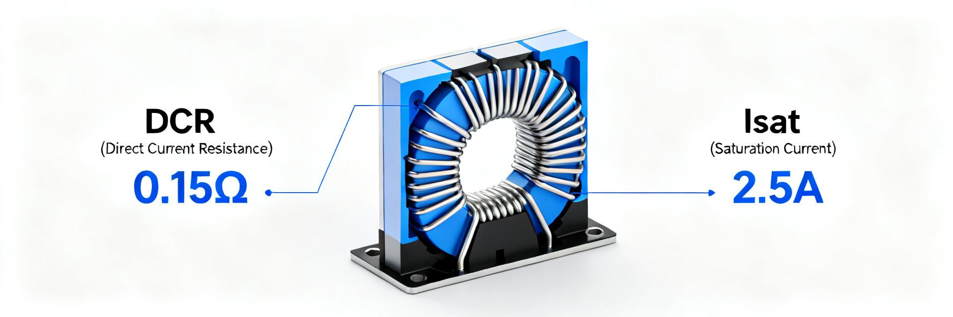
Point: Choose a part with appropriate current and thermal margins. Evidence: DC current rating, DC resistance (DCR), saturation current (Isat) and self-resonant frequency (SRF) define electrical and thermal behavior. Explanation: For DC‑DC converters, derate rated current by 20–30% for continuous operation; select DCR low enough to limit I²R heating and Isat above the peak transient current to avoid inductance collapse. Measure DCR on sample boards and verify inductance under DC bias before signoff.
Mechanical and packaging choices: SMD power inductor footprints & height
Point: Package size trades off current capability and board real estate. Evidence: Large-mass SMD power inductors (6–7 mm classes) typically carry higher current but increase thermal mass and solder requirements. Explanation: Choose low-profile variants when enclosure clearance and airflow are constrained; choose larger molded or multi‑pad flat-wire types when current and saturation margin matter. Consider board stiffening or glue for tall parts subject to vibration.
PCB footprint and land-pattern best practices for SMD power inductors
Recommended land pattern, pad design, and solder mask
Point: Pad geometry and solder mask control fillet formation and mechanical strength. Evidence: Use pads that extend beneath the part body to create full fillets; avoid overly large copper islands that prevent wetting. Explanation: Recommend pad length about 70–80% of body length on single‑end pads, with chamfered corners and a 0.5–1.0 mm paste-friendly aperture. Keep solder mask defined between pads to control fillet and prevent tombstoning; ensure robust fillet formation for shock resistance.
Thermal management on the PCB
Point: Thermals determine steady-state heating and converter efficiency. Evidence: Copper pours, thermal vias and trace widths affect dissipation and series resistance. Explanation: Place inductors away from hot MOSFETs and regulators; use exposed copper pours or thermal vias if the part dissipates significant power. Increase trace width and add vias for high-current paths to reduce I²R heating; ensure airflow paths are not blocked in the enclosure.
Soldering process: reflow profiles, paste, and assembly flow
Reflow profile setup for 2.2uH inductors
Point: Large-mass inductors need conservative reflow windows. Evidence: Excessive peak temperature or fast ramps can cause poor wetting or pad lift. Explanation: Use a standard lead‑free profile with a controlled ramp (1–3°C/s), a 60–90s soak at 150–180°C, and a peak of 235–245°C for typical SAC alloys. For heavy SMD inductors consider a slightly longer soak or reduced peak to improve wetting without exceeding manufacturer Tmax.
Solder paste selection and stencil design
Point: Paste alloy and stencil apertures control fillet size and joint reliability. Evidence: Insufficient paste causes weak fillets; excessive paste causes bridging or tombstoning. Explanation: Use SAC305 or equivalent paste for production; for larger pads use 0.12–0.15 mm stencil thickness and step-down apertures with rounded corners to reduce paste slump. Checklist: verify paste volume on first article, inspect fillets, adjust stencil as needed.
Hand-soldering, repair, and touch-up tips
Safe hand-soldering technique and tools
Point: Proper technique prevents thermal shock and magnetics damage. Evidence: Heat and flux choice determine joint quality and core integrity. Explanation: Use a temperature-controlled iron at 350–380°C with a medium chisel tip; use rosin‑based flux and preheat the board locally when possible. Tack one pad first, then the opposing pad, reflow both to form full fillets, inspect under magnification and clean flux. This soldering guide minimizes thermal stress and preserves inductance.
Removing and replacing a mounted 2.2uH power inductor
Point: Safe desoldering avoids pad lift and core damage. Evidence: Hot-air rework or dual‑iron methods are common. Explanation: Use hot air at controlled temps (220–260°C) and preheat; lift once solder flows. For iron removal heat both pads and lift quickly. After replacement verify fillet quality, measure DCR and inductance, and inspect for pad integrity and mechanical seating.
Real-world failure modes and troubleshooting
Electrical symptoms and root causes
Point: Temperature, noise or instability point to specific root causes. Evidence: Excessive temperature, audible buzz, inductance drift, and converter instability commonly trace to solder or spec mismatch. Explanation: Check for high DCR, saturation under DC bias, poor solder joints, or insufficient cooling. Use DCR meters, LCR under bias, and thermal imaging to identify hot spots. Correct by selecting higher Isat, improving pads or cooling, or redesigning current paths.
Mechanical failure cases and fixes
Point: Mechanical faults often originate from poor fillets or proximity issues. Evidence: Insufficient fillet, close placement to tall parts, or lack of board support cause cracks and lift. Explanation: Fix by redesigning footprint for larger fillets, adding glue or structural support, increasing standoff, and confirming reflow parameters. Add AOI/X‑ray checks to catch early mechanical defects before volume runs.
Mounting best practices & checklist for production readiness
Pre-production checklist (layout to assembly signoff)
Point: A short pre-production sequence prevents escapes. Evidence: Cross-functional signoff reduces rework. Explanation: Checklist: review spec sheet and derating, validate PCB footprint, run stencil and paste trials, perform one reflow trial with thermal measurements, verify DCR/inductance post-reflow, and execute vibration/shock checks for mechanical robustness. Use clear go/no‑go criteria for assembly signoff.
Long-term reliability & inspection
Point: Sample testing ensures field reliability. Evidence: Thermal cycling and vibration reveal latent issues. Explanation: Recommend sample plans: thermal cycling, vibration, solder fillet AOI or X‑ray targets, and in‑circuit DCR/inductance checks. Define pass/fail limits (e.g., DCR change
Summary / Conclusion
Recap: pick a 2.2uH power inductor with adequate current and saturation margin, implement an optimized SMD land pattern and paste stencil, use a slightly conservative reflow profile for large-mass inductors, follow safe hand-solder and removal steps, and validate through a brief pre-production checklist. For a reliable launch, run a quick pilot build and thermal check before full production.
Key summary
- Choose parts with DCR and Isat margins; derate continuous current by ~20–30% to limit thermal rise and avoid saturation for the 2.2uH part.
- Use defined land patterns with chamfered pad edges and appropriate paste aperture to form robust fillets for SMD power inductors.
- Adopt a controlled reflow profile and a paste stencil tuned to part mass; validate with a pilot run and thermal imaging.
Frequently Asked Questions
Will reflow damage my 2.2uH power inductor?
Reflow will not damage a properly specified inductor if you adhere to the vendor Tmax and use a controlled profile. Large-mass SMD inductors benefit from slightly extended soak or reduced peak to ensure wetting without overheating. Verify with a sample reflow and check DCR/inductance post-process.
How to reduce audible buzz or noise from a 2.2uH inductor?
Audible noise often stems from mechanical vibration or core magnetostriction under varying flux. Fixes: ensure solid solder fillets, add structural adhesive if needed, minimize stray fields by component placement, and verify operating flux density is below audible excitation thresholds by checking Isat and switching ripple.
What are quick checks after hand-soldering a 2.2uH inductor?
Inspect fillets visually and with magnification, measure DCR and inductance under expected DC bias, and perform a thermal scan at load. Confirm mechanical seating and absence of flux residues. If values drift beyond tolerance, rework and reassess footprint or part selection.